The slew rate in my application is slower than the value stated in the data sheet of the op amp. Why is this happening?
Read [FAQ] below or read application note here ; [APP] Ramping Up on Slew Rate
This thread has been locked.
If you have a related question, please click the "Ask a related question" button in the top right corner. The newly created question will be automatically linked to this question.
The slew rate in my application is slower than the value stated in the data sheet of the op amp. Why is this happening?
Read [FAQ] below or read application note here ; [APP] Ramping Up on Slew Rate
Ramping up on slew rate
Slew rate is the op amp’s fastest output voltage change over time, usually measured in units of volts per microsecond V/µs; however, some lower power op amps express slew rate in volts per millisecond V/ms. The data sheet slew rate (SR) parameter is the rate of change of the output voltage with a large input signal and unity gain setup (unless specifically stated otherwise). This single value is often the only obvious information about slew rate in the data sheet. It is important to know that not all applications will experience this magnitude of slew rate. Additionally, it is important to note that slew rate is not a constant value for all inputs and configurations.
Virtual zero and slew rate
Op amp circuits are easy to create and understand due to the ‘virtual ground’ mental concept. In closed loop circuits, the op amp’s large gain drives the input voltages to be the same. Input voltage difference (VID) is assumed to be zero. This assumption makes op amp circuit math simple. There are three effects that degrade this virtual ground concept in reality. First effect is DC offset voltage (VOS). The second effect is small signal gain; VID for small signal is simply VOUT divided by AOL (open loop gain). The third effect is slew rate generation. Only slew rate will be discussed in this application note. VID must be non-zero to generate slew rate. The greater the VID, the greater the slew rate. At some point, further increase in VID no longer increases slew rate. The data sheet value is the slew rate where further VID has no effect.
Bipolar in-depth example, SR is related to VID
Many bipolar op amp input stages simplify to this circuit seen in Figure 1. The VID, [IN+]-[IN-] voltage, controls how the bias current (B) is split between current paths I1 and I2. Current I1 is mirrored 1:1, to create an output current, I2-I1, that can vary from -B to +B. This output current charges the compensation capacitor (CC) and this charge rate is inverted to become output slew rate.

Figure 1
Therefore, the output slew rate (SR) can be varied from -B/CC to +B/CC. The result of B/CC is the slew rate that is specified on the datasheet. For some op amps, the positive and negative slew rate may be a little different; in this case the slower rate is recorded. SR in data sheet is always the magnitude of SR, ignoring polarity.
Current B and capacitance CC are different for every bi-polar op amp. However, the relationship between VID and ratio SR / max SR is similar for most. Slew Rate Scale (SR/SR[max]) versus VID chart data in Figure 2 applies for most bipolar input stage op amps. This consistent relationship is based on two formulas; VID = kT/q*ln(I1/I2); where k = Boltzmann’s constant, T = Temperature (Kelvin), q = Electron charge. The second formula is the percentage of full slew rate being |I1-I2|/(I1+I2).
Zero slew rate (0%) occurs when I1=I2 at VID=0 (more accurately stated as VID = -VOS). Maximum slew rate (100%) occurs when one of [I1 and I2] are zero and the other is at full current. This requires |VID| >> 100mV. Figure 2 show the relationship between VID and slew rate relative to maximum slew rate for most bi-polar op amps.
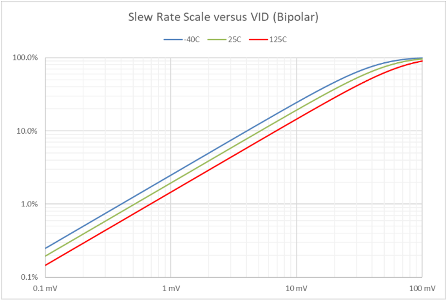
Figure 2
Figure 2 also applies to Darlington Bipolar input stages that have current sources on all emitters. There are a few Darlington op amps without a current source on the first emitter. TS321 is such a device; for this op amp, the VID needs to be the chart value doubled. For example, 2mV (1mV*2) gives 2% of full slew rate. For JFET device such as TL074, the VID needs to be eight times bigger; it takes 800mV to get full slew rate.
CMOS op amp slew example
CMOS op amp simplified circuit is the same as the bipolar example with CMOS transistor(s) as T1 and T2 in Figure 1. Drain current difference is based on voltage difference squared plus a linear factor. Therefore, expect some variation between different CMOS op amps. TLV9001 data is charted in Figure 3 up to 200mV; the curve looks similar to the bipolar example for VID up to 100mV. Most other CMOS amplifiers will show similar behavior. Figure 3 will be referenced several times later in the FAQ.
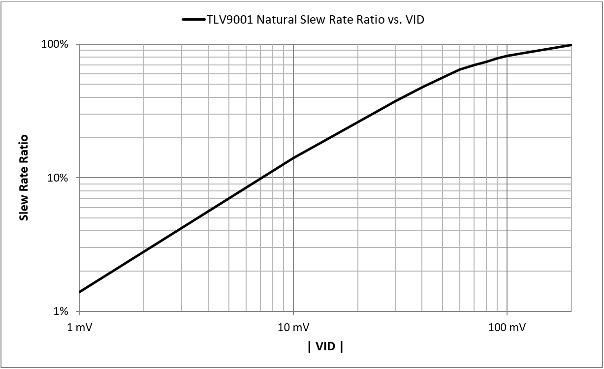
Figure 3
For TLV9001, 100% of the maximum slew rate occurs with VID >200mV. However, the internal bias current (B) and CC capacitor give 0.5V/us slew rate, not the 2V/us stated in the data sheet. This is because the TLV9001 employs a slew boost circuit to raise slew rate to 2V/us. Figure 3 is the ‘natural’ slew rate based solely on bias current and compensation capacitance with the boost circuit inactive.
Slew Boost Example 1
The simplified slew boost circuit in figure 4 will increase the capacitor charge current beyond the bias current level when VID becomes large enough. The boost circuit amplifier has a dead band with zero output current while input VID is low. At some greater VID, the boost current (IB) will rise with the VID input. This extra current increases the slew rate considerably. The boost circuit can provide positive and negative current flow to boost both positive and negative slew rates.
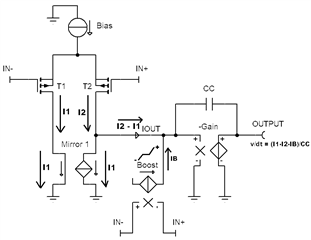
Figure 4
The boost current (IB) versus VID may be proportionate or it may be stepped at a certain VID level. TLV9001 employs both methods in figure 5. Negative SR boost (blue) increases proportionately starting near -140mV. Positive slew rate boost (green) increases suddenly near +270mV then raises proportionately. Regardless of the boost type, there is a limit to the boost current output. For very large VID, slew rate will become a fixed value. In TLV9001 example, the slower SR is about 2V/us, which matches the data sheet value.
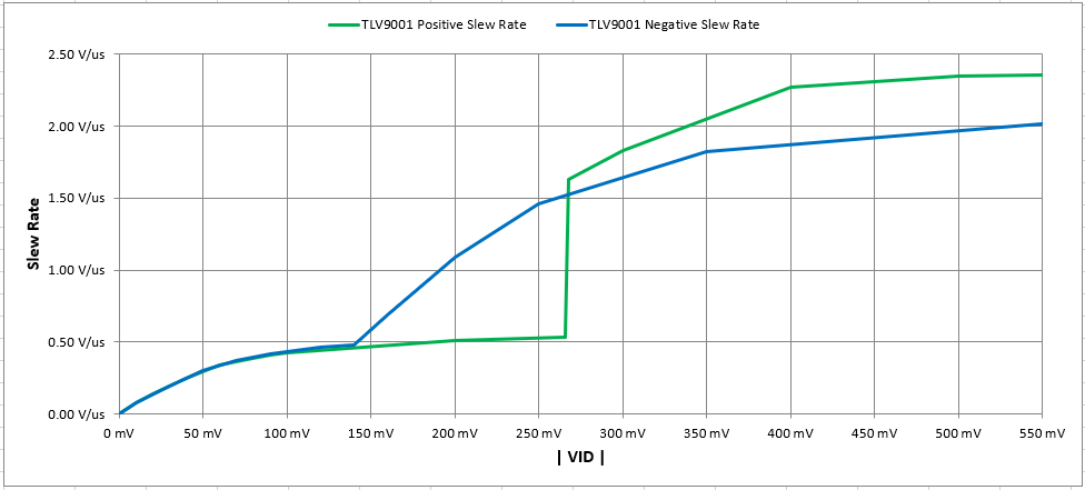
Figure 5
Slew Boost Example #2
OPA992, OPA2992, OPA4992 also have slew boost, but the slew boost occurs much earlier than TLV9001. Around 60mV, the slew boost engages starting with a lower initial slew rate. With further VID, the slew rate increases to 32V/us by VID = 800mV. Figure 6 and figure 7 show two views, log and linear scales, for OPA992 slew rate versus VID.
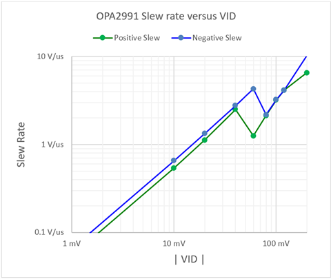
Figure 6
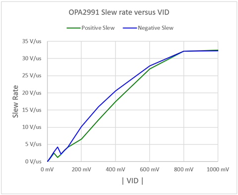
Figure 7
Four ways to determine boost or no boost using the data sheet
(1) Compare slew rate (SR) in V/µs to bandwidth product (GBWP) in MHz
|
Boost |
No Boost |
|
TLV9001 |
LMV831 |
Table 1
(2) Compare quiescent current (IQ) per channel to other op amps that have the similar supply voltage maximum and similar slew rate
|
Part number |
Iq per CH |
GBWP |
SR |
Related Features |
|
TLV9001 |
0.06 |
1 |
2 |
|
|
OPA345 |
0.15 |
3 |
2 |
Decompensated |
|
LMV831 |
0.25 |
3.3 |
2 |
|
|
LMV821-N |
0.30 |
5.6 |
2 |
|
|
OPA377-Q1 |
0.76 |
5.5 |
2 |
|
|
OPA376-Q1 |
0.76 |
5.5 |
2 |
|
|
OPA377 |
0.76 |
5.5 |
2 |
|
|
OPA376 |
0.76 |
5.5 |
2 |
|
|
TLV376 |
0.82 |
5.5 |
2 |
|
Table 2
(3) Find any large signal chart that has abrupt changes is rise and fall slopes.
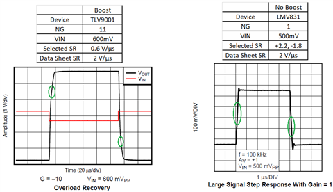
Figure 8
(4) Determine SR in small signal charts.
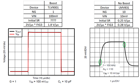
Figure 9
Slew rate dependencies on circuit signal levels and op amp gain set by feedback network
Figure 10 has two schematics that produce a 1V output step. On left, 1V is amplified by 1 and on right, 10mV is amplified by 100.
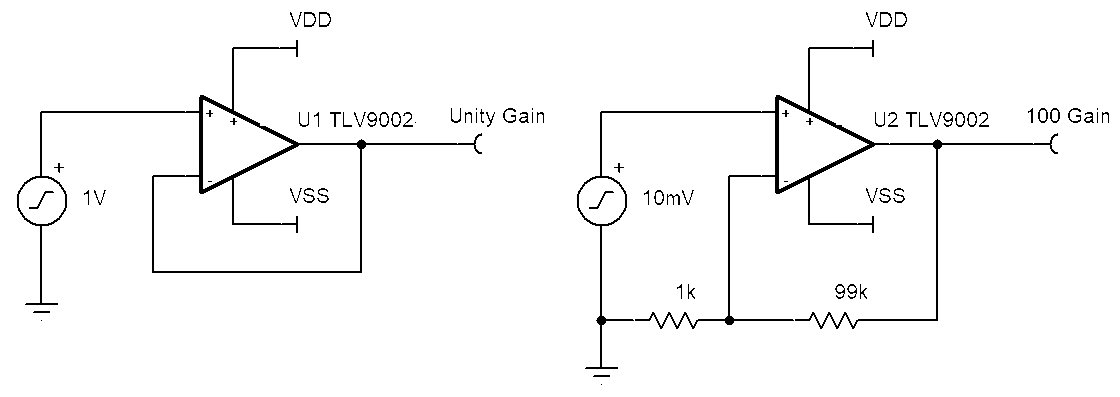
Figure 10
Figure 11 is the resulting simulation waveform from the Figure 10 schematics. The red curve is the unity gain setup. The red curve rises at 2V/us, same as the data sheet specification. The green curve has a slower slew rate that continues to decrease as the voltage rises. The initial slew rate for a 10mV input step, per Figure 3, is 14% of natural slew max of 0.5V/s which is 70mV/us. By the time the waveform rises half way, the VID has dropped to 5mV. Now SR is 7% (of 0.5V/us) 35mV/us
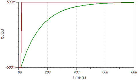
Figure 11
Even if TLV9002 didn’t have slew boost, the unity gain slew rate (0.5V/us natural) would be much faster than G=100 curve. Slew boost or not, a smaller input signal with higher gain will always have a slower slew rate than a larger input with lower gain.
How much output slew rate is needed to support a sine wave or other non-step inputs?
The peak slew rate of an output sine wave of frequency (f) and a peak to peak voltage (VPP) is SR = VPP * π * f. If the op amp slew rate is not high enough, then sine wave becomes triangular with a reduced amplitude. For any output waveform, the slew rate is simply the first derivative of the waveform. From these methods the required slew rate can be determined.
For signals other than a step input, also consider gain bandwidth product (GBWP). The absolute minimum GBWP needed for an application is [Frequency maximum] * [Noise Gain]. For small signals on slew boost devices, it is best to use only GBWP for determination of sufficient op amp speed for small input.
With required SR & GBWP determined, consider how much of the input signal can be assigned to be used as VID to generate that slew rate and gain. Choosing an op amp with much greater SR and GBWP will reduce VID required and potentially reduce distortion. Higher SR and GBWP come with higher quiescent current. For low power applications there will be a compromise between supply current and AC performance.
Stability also plays a role in observed slew rate and closely and inversely related rise time.
Very stable circuits with 90 degrees or more phase margin will have longer rise times with slower observed SR because feedback is fully negative. The advantage to very stable circuits is the lack of overshoot. Critically stable and poor stability circuits with 45 degrees or less phase margin have a significant positive feedback effect that shortens edge times and increases observed SR at the expense of having overshoot, ringing or possible oscillation.
Summary
The slew rate parameter in data sheet is the typical fastest possible output rate change in V/us. Slew rate in small input and high gain applications will be reduced. Input difference voltage, VID is needed to achieve an output slew rate. Faster SR requires more VID. More VID makes the virtual zero op amp concept less true, so distortion may also increase. It is best to select an op amp with much higher slew rate and bandwidth than needed for lower signal distortion.
Additional Resources
TI precision labs detailed slew rate information: TI Precision Labs - Op Amps: Slew Rate Introduction
Application Report: Understanding Operational Amplifier Specifications. See sections [4, 4.1, 5.13]
TI precision labs basic slew rate information: https://training.ti.com/ti-precision-labs-op-amps-slew-rate-lab