This thread has been locked.

If you have a related question, please click the "Ask a related question" button in the top right corner. The newly created question will be automatically linked to this question.

OPA548: current booster design and stability

Part Number: OPA548
Other Parts Discussed in Thread: OPA192, CSD18540Q5B

Hi, 

We are trying to design a current amplifier with the following requirements: 

- An AC signal, isn't necessarily a sinusoidal. 

- 10V <=Vout<=16V @ 15HZ - 15KHZ (or as close to this full frequency range as possible).

-Our current demand is 30A max. 

The simulation results indicate that the design might be able to work with the proper output capacitance compensation (the circuit is supposed to drive one of our boards which has a high input capacitance, that I added to the output in the attached simulation model).

The Data Sheet of OPA548 doesn't specify the output resistance of this op-amp and I'm not sure that the simulation takes into account the exact output resistance. Even if it does, I prefer not to guess the exact capacitor and resistor that should be added as an in-loop compensation. 

can you please suggest the compensation values for this circuit or provide a PN of more suitable op-amp for our design? 

Thanks!

Anna

currentbooster.TSC

  • Hi Anna,

    The Data Sheet of OPA548 doesn't specify the output resistance of this op-amp...

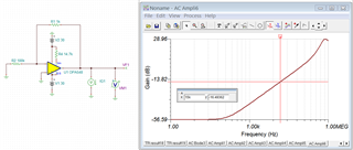
    The OPA548's output impedance is very small, which is Zo_ol/(1+T), where T is the loop-gain or β*Aol. In this configuration, the closed loop Zo is approx. -16.5dB or 0.15Ω @15kHz. 

    OPA548 Closed Loop Output Impedance.TSC

    - 10V <=Vout<=16V @ 15HZ - 15KHZ (or as close to this full frequency range as possible). can you please suggest the compensation values for this circuit or provide a PN of more suitable op-amp for our design? 

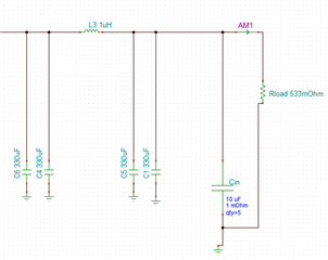
    What is the actual load? Is it 1Ω? As it is configured, the output has a Q of 20dB at approx. 5.25kHz due to 1/(2*pi*sqrt(LC)), the the output's frequency starts to attenuate after the double pole of 5.25kHz at -40dB/decade. So it will attenuate approx. -17dB or 0.141*Vin at 15kHz. (The simulation is expanded qty=5 10uf, 1mΩ ESR capacitors). 

    OPA548 LCR load 11222021.TSC

    If you want to clarify your actual load, and design requirements, I can put together a compensation scheme and check out the loop stability in a circuit. Yes, it should work. 

    BTW, you do not have to use OPA548 for the application. You may use any 36V precision op amp with low Vos for the driving application. If the application has to drive large capacitive or complex load, I would mirror the current on left side of V-to-I branch, and drive the capacitive load on the 2nd branch or stage, which is similar to the link below. Op amp does not like to drive large capacitive load, which it will create additional pole in a closed loop and result instability of op amp. 

    https://www.ti.com/lit/ug/slau502/slau502.pdf?ts=1637598438660&ref_url=https%253A%252F%252Fwww.google.com%252F

    Best,

    Raymond

  • Hi Raymond, 

    Thank you very much for this detailed response. Our current load in the system is somewhere between 20A -30A max, so we need this design to work for a current as high as 30A. I only simulated it with 1ohm load to see how it reacts with a lower current load, and apparently the results are worse than the results of the simulation I made with 500mohm load resistance in terms of output stability. If you can put together a compensation scheme is would really be a great assistance for us.  In general, if the compensation can work for our whole span of frequencies (15Hz-15Khz), it would be amazing , though I'm not sure it's possible.

    Meanwhile I'll try to simulate the other option you suggested, does it replace entirely the need for a compensation network? 

    By the way, the BJT we are gonna use can be replaced as well. Do you have a High power, High voltage option that we can acquire? I think it's better if the transistor will be suitable for high temperatures as well, because of our high power application. 

    Best regards,

    Anna

  • Hi Anna,

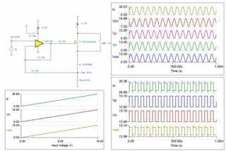
    Enclosed is an example of up to 30A V-to-I converter. The circuit is compensated and it is stable up to 15kHz or higher. The BW of the circuit is approx. 115kHz with phase margin of 60.5 degree. 

    currentbooster E2E Transient 11223021.TSC

    The BJT we are gonna use can be replaced as well. Do you have a High power, High voltage option that we can acquire? I think it's better if the transistor will be suitable for high temperatures as well, because of our high power application. 

    Yes, all the components in the above circuit may be altered. For instance, we can replace OPA548 with OPA192 or similar low Vos precision op amp. We can replace BJTs with MOSFETs, and reduce 5 BJTs to 2 or 3 Mosfets to simplify the design. We may even lower the supply voltage slightly to reduce the power dissipation at the transistors etc.. 

    I do not know what components you have in hand, so I am using the parts you provided. Please let me know the type of application you are working with, and we may take the approach from there. 

    Best,

    Raymond

  • Hi Anna,

    Here is an alternative V-to-I driving circuit as an example. It may simplify your design. 

    OPA192 Currentbooster E2E Transient 11242021.TSC

    Without knowing your specific requirements, I did not spend a great deal to optimize this. For instance, if you use OPA192 or similar precision op amp as V-to-I converter, then you can simplify the op amp driving circuit. OPA548 is designed for driving high current application directly. You may also simply BJT design, where I selected one of our mosfet drivers. You may need to parallel multiple MOSFETs in order to reduce heat dissipation and use heat sink/air flow to lower its heat dissipation. 

    Below is a link in selecting the N-Mosfet driver.  

    https://www.ti.com/power-management/mosfets/n-channel-transistors/products.html#p267=40;110&p2748=0.82;500&sort=p267;desc

    If you have additional questions, please let me know. 

    Best,

    Raymond 

  • Hi Raymond,

    Thank you very much for the detailed response. This is going to be an addition to our test equipment, so the application is going to be lab testing. 

    I guess it should be automotive because of the high output power, so it's important that all the components have a high power dissipation property and low resistance. 

    Are the alternatives you provided suitable for our high output power? Do you believe that one FET is sufficient? the reason why we wanted to work with multiple BJTs is that we wanted to split the current between them and we don't have an issue with space (because it's a board for testing purposes).

    Best regards, 

    Anna

  • Hi Anna,

    Are the alternatives you provided suitable for our high output power? Do you believe that one FET is sufficient?

    One mosfet will not be handle the heat dissipation for 30A load application. Under a static load application, say Vin=13V @30A, the voltage across the transistors (BJTs or MOSFETs) will have 7V drop with 20V supply rail. The heat dissipation across the transistors V*I = 7V*30A=210W, which will be an issue.

    Regardless what you are going to use in BJTs and MOSFETs, you may consider to lower the supply voltage to reduce the heat dissipation at the transistors. Yes, you will need multiple BJTs or MOSFETs to work around the application, and you will need to implement heavy duty heat sinks + air flow/liquid cooling block etc.  to lower the transistors' operating temperature. 

    If you are able to provide me the worst case scenario, I can simulate it and provide some recommendation. Since this is a lab application, it will be good to handle the application with excessive cooling (It is likely that your worst case scenario will dissipate a significant amount of heat across the transistors, close to 200W+). If you are able to lower the 20V supply rail, say 17Vdc, you will reduce the heat dissipation from 210W to 120W as the example above, which is a lot easier to manage.  

    It will be good ideas to replace OPA548 with OPA192 or similar precision op amp for the application. OPA192 is RRIO op amp and will work with lower voltage rail for controlling the V-to-I application. 

    Best,

    Raymond

  • Hi Raymond,

    The signal that this circuit will produce is a 10V-16V sine wave. The supply voltage is directly from a power supply, so it shouldn't be a problem to lower it - but the highest voltage the signal reaches is 16V  so the supply voltage needs to be high enough to keep the BJTs/FETs always open (while using the test board). The test itself shouldn't take longer than 1 minute. What are your suggestions in this case? If you need more information don't hesitate to ask, your input is very helpful for us.  

    Thanks,

    Anna

  • Hi Anna,

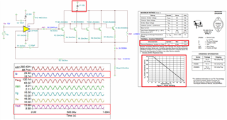
    If you are doing a test board in a lab, I do not see advantages to make any changes.  Assumed Pavg = 110W over 5 TO-3 BJTs, each will dissipate approx. 22W. With Junction to case temperature of 0.5C/W, the junction temperature will increase 11C from room temperature. I will recommend to use a single heat sink plate for the TO-3 mounting, if you have these, even it is operating for short duration.   

    Pavg currentbooster E2E Transient Avg Pwr 11272021.TSC

    If the application will be placed on PCB (in SMD), then OPA192 + NMOSFET design have some advantage due to its compact size. You are unable to replace OPA548 with OPA192 in BJT drivers, since the op amp is required to drive larger Vbe current. 

    If you have additional questions, please let me know.

    Best,

    Raymond

    Pavg OPA192 Currentbooster E2E Transient 11272021.TSC

  • Hi Anna,

    I am going to close this inquiry. If you have additional questions, you may still re-open the thread or create a new one via E2E. 

    Best,

    Raymond

  • Hi Raymond, 

    I'm Sorry for the late response - I wrote you a response and apparently it wasn't sent. We really appreciate your help and your implementation is already in the process in our team, you really helped us a lot. If you have an application note or your personal calculations for the compensation detailed, please share it here. We tried to come up with compensation values before using your assistance but we couldn't get the output as stable as you provided.

    Best Regards, 

    Anna

  • Hi Anna,

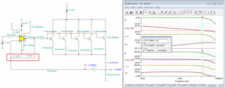
    Enclosed is the small signal injection model that my compensation is based on. You can compute the compensation values of R1 and C1 and check for the loop-gain stability. NPN 863-2N5686G PSpice model model, is what I use from the get-go. 

    currentbooster E2E AC Analysis 11302021.TSC

    Below is the model with OPA192 and CSD18540Q5B N-Mosfet. Since I do not know what you are using, I attached both in the reply. 

    Pavg OPA192 AC Analysis E2E Transient 11302021.TSC

    If you need further assistant, please send me a scope shot which it may help. I have pretty good confidence in TI's PSpice model, but I am unable to say about 3rd party ones. 

    Best,

    Raymond

  • Hi Raymond, 

    Thank you for sharing this. I have a problem with connecting your model to our input filter, that was connected in the initial simulation file that I have sent you. The resistance load is not constant as I said but the filter is very real and it was what we have in our board, which this one needs to drive.it seems to not provide the 10V-16V ripple we need.

    1374.currentbooster.TSC

    Best Regards, 

    Anna

  • Hi Anna,

    I need to know what is your load. My previous circuit is assumed that the load is resistive in nature, which is 533mΩ. You are using the 533mΩ load to generate a constant current up to 30A. 

    If the load is shown below with large C, L and R, then the driving circuit will not work for the application. This is a complex load and op amp is unable to drive the such load directly with the circuit that I provided (>15kHz BW). The following circuit is a complex load. 

    BTW, if the above circuit is the actual load, the Rload frequency is only able operate up to 5kHz (see my previous replies). The output starts to attenuate after 5kHz.  

    In the previous reply, I mentioned the following circuit. If the above load is complex, then you have to use similar circuit (see below) to create a current mirror on a second stage to drive the load up to 30A. Please let me know what is your load characteristics in L, R and C. 

    Best,

    Raymond

  • Hi Raymond,

    Our capacitance load is exactly what the simulation file has, meaning 1370 uF.

    The inductance is 1uH.

    I don't have a constant resistance value to give you, the output of the circuit should work for up to 30A. 

    What are your suggestions in this case? if it will work up until 5kHz it might be good for us too.

    Thanks, 

    Anna

  • Hi Anna,

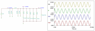
    Based on your description, you want to drive the following load up to 30A as shown in the simulation below. In other words, the load is NOT a constant current source. The input voltage, VG1 as simulated is from 10V to 16Vdc, and the output of the complex load swings from 18.53A to 30A. 

    OPA548 Driving Complex Load 12012021.TSC

    Enclosed is the load simulation. Please let me know if I understand the requirements correctly. 

    Best,

    Raymond

  • Hi Raymond,

    Yes, this is correct. The swing of the current will be probably lower, from about a bit higher the 20A to a maximal current of 30A, but It shouldn't influence the design other than the fact to the load is not constant and the amplifier should be able to drive up to a 30A current.  Other than that, you understood the requirements correctly. I'm sorry if I wasn't clear enough before that.

    Thanks, 

    Anna

  • Hi Anna,

    After I understand your requirements, I found that the op amp with current booter circuit is unable to drive such large 1320uf capacitive load. In other words, the op amp will not be stable and I am unable to compensate for the large capacitive load. Even I am able to find a compensation solution, the compensation will be used up the most of the required 5kHz bandwidth.  

    If the OPA548's driving circuit is able to bypass the π filter at the load as shown above, I may give a try in OPA548, but I am not making any promises. 

    In such a load application, it is typically done via DC/AC converter. On the DC side, power input driver has to generate PWM modulated sine wave at high frequency, and π filter will filter out the harmonics and generate the required sinewave via LPF. 

    If you have additional questions, please let me know. 

    Best,

    Raymond 

  • Understood, thank you very much again for your assistance - it wasn't trivial at all and we really appreciate the effort. 

    Unfortunately we can't bypass the filter. We will explore an option for a suitable testing equipment instead. 

    You can close this thread. 

    Best regards, 

    Anna

  • Hi Anna,

    You are welcome. 

    If the application is unable to bypass the filter with the large capacitive load, you are unable to drive the application with Power Op Amp or Op Amp + Current Booster. As I suggested, the pi filter is likely used to remove switching harmonics and filter out modulated PWMs in DC/AC converter.  

    If you need further assistant, please let me know. 

    Best,

    Raymond

  • Hi Raymond,

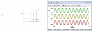
    we decided to remove 2*330uF from our load (as you can see in the attached simulation file). Now, in the steady state, it works nicely. 

    Do you think that the BJTs will be able to share the current pretty much equally even without the 20mohm emitter resistance? 

    The problem is that those resistors should be very high power rated and the power dissipation capabilities will go down when the temperature rises.   

    7180.currentbooster.TSC

    Thanks!

    Anna

  • Hi Anna,

    Do you think that the BJTs will be able to share the current pretty much equally even without the 20mohm emitter resistance? 

    You may remove these resistors; the most of voltage is going to drop across Vce anyway. The heat dissipation of 20mohm resistor is approx. 4^2*0.02Ω = 0.32W, @20A of total load. If you keep all the transistors on a single heat sink plate, they should share the current better. 

    Regarding to the op amp stability after 2x330uf capacitors are removed, I do not believe that the circuit is stable. Yes, it would operate better than before, but the circuit still does not have the required the phase margin (>45 degree). The oscillation will show up if input is operating in square wave, step function or there is load pulse at the output etc.. 

    Best,

    Raymond

  • Hi Raymond, 

    You are right - it works only for specific frequencies and still unstable for others. 

    Other than that, unfortunately we cannot remove the whole filter.

    Thank you for  the quick response. 

    Anna

  • Hi Anna,

    Please try to insert 5kΩ as shown below. It will stablize the circuit better, say if frequency is greater than ~1kHz range. So the circuit will be stable if the application is operating at higher frequency. The output signal will start to attenuate after approx. 6kHz range. 

    If input signal frequency is low, say <500Hz, you may see oscillation, but the circuit will work conditionally. This is due to the LC filter in series with the load.  At low frequency. 1uH is closed to be a short and that will place 600uf capacitive load at the output, which it will introduce another pole within the feedback of the closed loop.  

    Best,

    Raymond

  • Hi Raymond, 

    For f=5k is seems that the opamp can't drive the load, it requires too much current and the opamp reaches it's limits and goes into saturation.  Unfortunately, the load is very small at this frequency because of the filter - so it requires too much current. The output current in this case is undesirably very large, much larger than 30A.

    We very much appreciate your help on this design. 

    Thanks, 

    Anna 

  • Hi Anna,

    For f=5k is seems that the opamp can't drive the load...

    The suggested circuit is very similar to what you have. 5kΩ or 10kΩ is the circuit feedback resistor. I am suggesting 5kΩ to provide you with higher BW. 10kΩ should work as well with lower BW (approx. 70-80kHz range if I recalled correctly).  

    Regarding to the frequency response of the circuit, LC filter determines where the attenuation is going to be or 1/(2*pi*sqrt(LC)).  

    Best,

    Raymond

  • Hi Anna,

    I hope that you have found a solution to drive your application. 

    I am going to close this inquiry. If you have additional questions, please let me know. 

    Best,

    Raymond