- Ask a related questionWhat is a related question?A related question is a question created from another question. When the related question is created, it will be automatically linked to the original question.
This thread has been locked.
If you have a related question, please click the "Ask a related question" button in the top right corner. The newly created question will be automatically linked to this question.
Hello,
How to set the Rf and Rg resistor of THS4503? I need to change the 1.0~2.3V input to each -0.05~1.95V output of THS4503, and the output common mode voltage is 0.95V for the ADC.
Best regards
kailyn
Hello Kailyn,
These resistors are for gain setting, impedance matching, and balancing between the two inputs of the fully differential amplifier. Is the source 50 ohms? We can help calculate these resistor values, and also I can send over a new excel calculator that works out these values.
Is this differential to differential or single ended to differential? Also is the input range 1 to 2.3V and is the output range 0.05 to 1.95V? Are they looking for an attenuator type of application?
Thank you,
Sima
Hello Sima,
Yes, the source is 50ohm impedance. I remember there is a excel or software which could help to calculate the resistors, but I couldn't find it. Hope you could send it to me again. Thank you very much.
The application need single to differential. And it is right that input range 1 to 2.3V and is the output range 0.05 to 1.95V.
Best regards
Kailyn
In addition, each output( Vout+ and Vout -) THS4503 is -0.05 to 1.95V input. Because the Vicm of ADC is 0.95V, Vpp is 2V, so the input voltage range of ADC is -0.05V~1.95V.
Best regards
Kailyn
Well Kailyn, 1st lets confirm the design needs
Your ADC likely has 0.95V CM and 2Vpp max differential input - that then maps (remember differential input)
usually target max -1dBFS input or about 1.8Vpp differential max. Your input has a 1.3V single ended peak so you need a gain of 1.38 from the input termination. However, the 1.8Vpp swing is split between the two polarities so each output is 1.8Vpp/4 = +/-.45V around 0.95Vcm
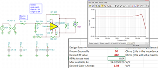
The old THS4503 might be a poor choice here as it is not RR out - most folks like to use a supply on the ADC driver as low as possible to reduce overdrive risk. I would consider the THS4541. From there, and simply using the 402 ohm feedback R in a lot of the datasheet, Here is a solution on 3.3V supply (once you get the desired output voltages on the output pins, you need to check CM and output stage headrooms, ok here using the THS4541 which is intended for this type of app. This is one of several calculators I had developed from the closed form soluations I had worked out quite some time ago - those equations are in the THS4541 datasheet. I had another one the snapped to E96 values with min error, not finding that one now.

Here is the file,
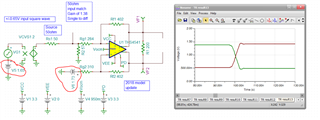
I went on to set up for you input swing, I added a 1.65V CM voltage on the signal source, I expected 1.65V at the Rt input point but get a 1.73V - not sure where that offset is coming in, but if I then add the required CM bias on the other side of the FDA, I get a pretty good output using 3.3V supply. This is I think what your ADC would like to see.
I am missing something still on why the midpoint input is not correct, but this is closer here, 10Mhz input square wave with 2nsec edges,

And the updated file,
Hi Michael,
Thank you very much for your reply.
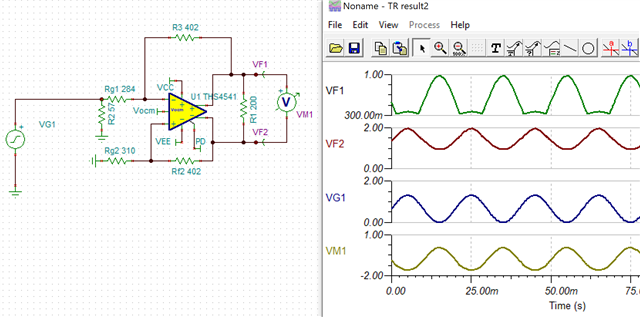
The first.TSC file,I don't know why I didn't get the simulation results with "Analysis-Transient". I build the circuit simply, and the results as as following:

In addition, could you please send me the excel calculator that works out these values? Thank you very much.
Best regards
Kailyn
As I simulated with the results, VM1 should be 0.05V~1.85V,1.8Vpp with 0.95V common voltage, but actual the VM1 looks like incorrect.
Best regards
Kailyn
I think I needed to add the CM input voltage on the Rg2 side, which I did and it works better - I think Simi was going to send you the TI calculator, mine includes industrywide parts and quite a lot of further noise analysis, and part select flows - but industrywide. If you start with the same Rf selections, the TI one shouid get to the same input and Rt values. Here is the original article, before then the solutions were iterative, but the quadratic here is exact. When I was testing this I was testing results against the ADI Diff-amp calculator which is out there as a public tool.
The original article is starting to dissappear as the original publishers dissolve, but I found a migrated version here, there is a part 2 also,
https://studylib.net/doc/18053452/dc-coupled--single-to-differential-design-solutions-using...
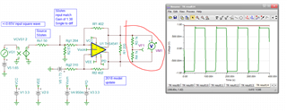
Use the 2nd file, yes, if you look at the diff output it should be 1.8Vpp, but you need to add a CM test point to see the 0.95V output CM. Just add 2 1kohm R's across the outputs to a midpoint and probe there for the CM level.
Here I went to a differential output probe and a CM probe on my square wave input, the diff output is indeed +/-0.9V and the red line at the top is the CM DC output of 0.95V - assuming this is getting closer, the next layers are to add any MFB active filtering in the FDA stage and interstage filtering to the ADC if need be - usually so.
