Other Parts Discussed in Thread: INA226
I Hope you are doing well.
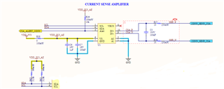
We are facing some issues with the I2C lines of INA226-Q1 IC.
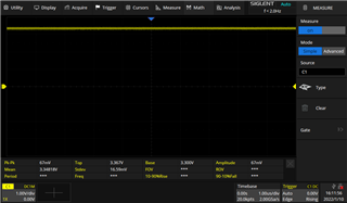
Kindly find the below image for reference. The below profile is captured across the Rshunt of 5mΩ but in our design we are using Rshunt of 0.5mΩ.

When we are getting the above profile across Rshunt of 0.5mΩ, we are able to see 100A charging and 84.3A discharging current through Rshunt.
Due to the above profile the following issues are observed
1.INA226 IC stops communicating with microcontroller..
2.SCL line is pulled to 3V3.
Kindly go through it and help us troubleshoot as early as possible.