This thread has been locked.

If you have a related question, please click the "Ask a related question" button in the top right corner. The newly created question will be automatically linked to this question.

INA2332: Offset is not constant among all channels even common mode input is also 0

Part Number: INA2332
Other Parts Discussed in Thread: INA332, INA2321

Hello I need help with the design

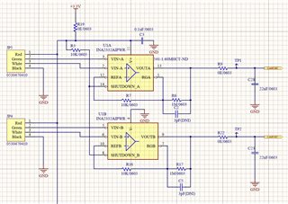
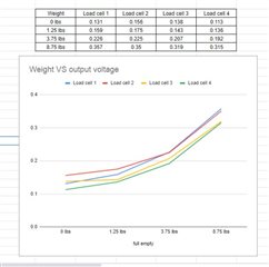
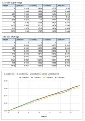
I am using 2 INA2332 IC for 4 load cells I want a gain of 500 so calculated resistors were R2= 1M and R1 = 10K 
Use the same type of resistors for all 4 channels in the output but I am getting an offset of 1.2V in one channel and 0.6V in other one 

I am ok with offset but it should be constant so that I can reduce it from the input by adding a resistor divider 

Things I tried 
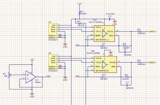
1) I tried grounding reference Ref A and Ref B 
2) I tried some more resistor combinations with it I could find more offset changes 


  • Hi Atharv,

    I see several issues:

    1. You cannot leave the REF pin unconnected. Connect it to midsupply, driven by a low impedance.

    2. 22nF is a way too high capacitive load. Increase R9 and R22 to 47...100R.

    3. Remember that load cells can show huge offset voltages.

    4. The input offset voltage of up to +/-9mV of INA2332 is also multiplied by the gain of 505, giving an offset voltage of up to +/-4.5V at the output of INA2332. You should decrease the gain or adjust the offset voltage.

    Kai

  • Hi Atharv,

    Thanks for your post. Kai's analysis is correct. On a single-supply application, it's recommended to connect this to mid-supply. This is explained further on page 10 of the datasheet. Please apply Kai's suggestions and let us know the feedback. 

  • Hii Kai & Tamara 
    Thanks for the help


    I made changes as suggested by you 

    Vref is set to mid-supply of 1.65V 

    Now I am still getting some differences my 4 channel voltages are 1.885V, 1.090V, 1.215V, 0.478V 

    I swapped the load cell from one channel 1 to channel 2 as for checking whether it is there from the load cell
    but still, the offset voltage of that channel remains the same 

    Also, the gain linearity is fine but can we improve it more I have attached an image for my results 


    Attached updated schematic 

  • Hi Atharv,

    as I already mentioned:

    4. The input offset voltage of up to +/-9mV of INA2332 is also multiplied by the gain of 505, giving an offset voltage of up to +/-4.5V at the output of INA2332. You should decrease the gain or adjust the offset voltage.

    So the differencies you see between the INA2332 channels come from the varying input offset voltages of the individual INA2332. Again, please considerably decrease the gain.

    Carry out the gain linearity analysis after reducing the gain. I'm sure you will see a better performance then.

    Kai

  • Hi Atharv,

    In addition to lowering the gain as Kai suggested, can you please clarify the voltages you are feeding into the INA? At any instant during the measurement, what do you see on IN+ and IN- of the INA? I would like to make sure that the input differential voltage AND common mode voltage are within linear range of this INA. 

    We have a calculator tool inside the Analog Engineer's Calculator called "INA VCM v VOUT". Here you can select the INA332, and enter your supplies, gain, reference voltage and common mode voltage. The calculator will output a boundary plot of the linear operating range including the allowable input differential voltage and expected output swing. 

    You can download the calculator here: https://www.ti.com/tool/ANALOG-ENGINEER-CALC 

    Once downloaded, click on the little + sign next to "Amplifiers and Comparators" and then click on "INA Vcm vs Vout". Here is a snapshot:

    Here I selected the INA332, with 3.3V single supple, 505V/V gain, 1.65V reference. I also "assumed" VCM to be mid-supply to allow for the widest input dynamic range, but this will depend on your specific input signal. Please determine this and enter the appropriate level. Assuming the above conditions, though, the allowable input differential voltage is -3.328mV to 891.098uV to yield an output of 0.025V to 2.1V.


  • I could see better performance 
    But what we can do to increase linearity between all amplifiers more 

    Somehow we need to make the line slope equal for all the load cells so that we can implement the calibration algorithm effectively 

    Sharing results of gain set to 95


  • Hi Atharv,

    unfortunately, load cells are well known for their huge offset errors, gain errors, linearity errors and part to part variations. In addition, some of them show relevant hysteresis errors.

    One remedy is to choose pre-calibrated load cells. But this can be very expensive. Or you calibrate them individually by hand, piece for piece.

    It is true that load cells can be calibrated by using trim pots in the bridge legs. But this method can result in big temperature drifts and is not recommended.

    The simplest way is to choose a low gain in the instrumentation amplifier to prevent signal clipping and to do all the calibration in the software.

    Kai

  • Hi Atharv,

    Kai's analysis and suggestions are correct. Please let us know how we can support you moving forward. 

  • Thanks for all the help Kai and Tamara 

    What if we go for INA2321 this has an offset of 1mV were as the current has an offset of 9mV?

    with it, we can at least reduce the initial offset 

    What is your recommendation?


  • Hi Atharv,

    yes, you can do that. But as being a micropower instrumentation amplifier the INA2321 shows considerable higher noise. This can be an issue when chosing a high gain. Also, for the same reason, the INA2321 is not as fast as the INA2332.

    Kai