This thread has been locked.

If you have a related question, please click the "Ask a related question" button in the top right corner. The newly created question will be automatically linked to this question.

OPA4322: TINA simulation as a DAC buffer (Unity gain buffer )

Part Number: OPA4322
Other Parts Discussed in Thread: TINA-TI

Hi OPAMP folks,

I'm doing TINA simulation with OPA4322 as an unity gain buffer. Could you help advise for its operation?

What I'm trying to do : 

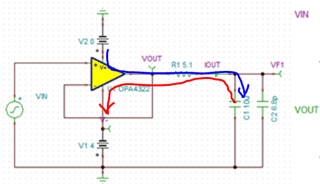
I want to implement an unity gain buffer (DAC output buffer) with OPA4322 to see how much of current is drawn from voltage supply during the DAC value change.

Condition : 

- Positive supply rail : GND

- Negative supply rail : -4V

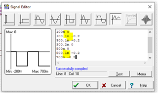
- DAC variation (△Vin) : 0.4V or -0.4V

- Cload and Riso : 10uF and 5.1ohm

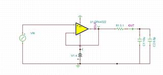
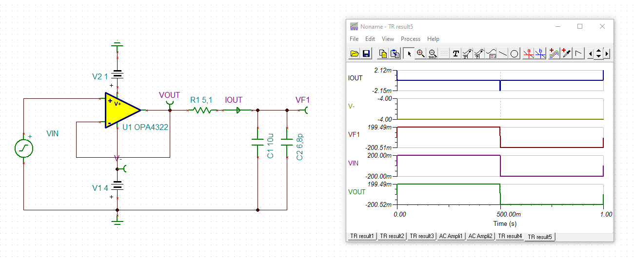
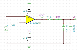
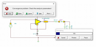
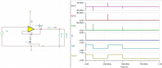
I configure the circuit as above. And I have questions as below from the simulation result.
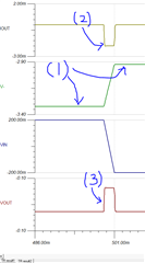
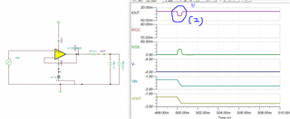
(3)

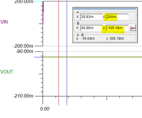
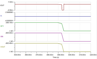
It looks the the unity gain buffer does not operate normal. As it's a voltage follower, I thought VOUT should follow the VIN. Is there anything wrong in circuit? 
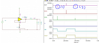
(1) 1.

Per my understanding, V- is supposed to stay in -4V under any circumstance. But it's not -4V during VIN = 0, and it's not -4V also during VIN=-0.4V. Could you advise why the V- node is not stable on -4V?

(1) 2.

Moreover, I do not understand how V- changes from -3.32V to -2.92V when VIN changes. Could you explain the mechanism?

(2) 1.

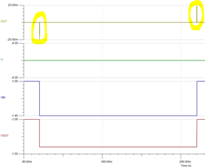
Per my calculation with the basic capacitor equation (I = C* dv/dt), 4mA of the instant current is required to charge 10uF capacitor on output.

I = 10uF * 0.4V/1ms = 4mA (1ms is set by myself from the input signal. Please find the VIN setting.)

But the simulation shows 2mA only. Could you advise why?

4375.OPA4332_DACBuffer.TSC

Thank you.

  • Hi Ella,

    the input signal violates the common mode input voltage range of OPA4322. Better, to add a small positive supply voltage to allow a small positive input voltage, like this for instance:

    ella_opa4322.TSC

    Also, the charging time is not 1ms but 2ms. This halves the charging current:

    Kai

  • Hi Kai,

    Thank you for the clear answer. Could you help answer on additional questions below?

    1. From your attachment, I remove positive supply and get a result as below : VOUT is saturated to positive rail while VIN is 200mV. 

    Per the result above, Vo has an approximately -105.18 mV of headroom. But the headroom specification in datasheet is max 30mV. Where does this difference come from?

    2. It may be going to be a very fundamental question... Basically, I'm doing this simulation to check how a negative power supply should be designed to drive high capacitive load on DAC output on my board.

    The negative current in the simulation is the current which flows into the buffer output (red arrow), while the positive current is the current which flows out from the buffer ( blue arrow). In the bench test, there might be a supply voltage drop if the positive current is too high - -4V supply may drop to -3.xx or -2.xx. I wonder what happen to the supply voltage when the negative current flows. I don't think the -4V supply may go up to -5.xx or -6.xx. Could you advise what would happen?

    3. When I apply the input voltage with 100us of rising/falling time, it comes up with convergence problem. Could you advise why this error occur? Is it just the tina software cannot support the sharp edge? To avoid this problem, how much of rising/falling time should be secured?

  • Hi Ella,

    again, the input voltage must not lie outside the supply voltages by more than 100mV:

    But this is the case, when inputting a signal which is 200mV more positive than the positive supply voltage:

    A positive supply voltage of more than 0.1V would do the trick:

    To your second question: If the load current spike is only shortly lasting, it will be fully supplied or absorbed by the decoupling cap. Longer lasting current spikes have to be supplied or absorbed by the supply voltage regulator itself. Supply currents of the proper sign are no problem for a voltage regulator. Reverse currents, on the other hand, can usually be absorbed, if the total supply current drawn by the circuit is higher than the reverse current to be absorbed.

    As an example: If the total supply current supplied by the regulator is 100mA, then about 100mA reverse current can be absorbed.

    If your reverse current is higher than the total supply current supplied by the regulator, a dummy load can be installed to increase the total supply current. Or a special voltage regulator can be used, which can absorb the reverse current.

    The voltage regulator in the simu, as being an ideal voltage source, can usually supply and absorb any current without going into trouble.

    For clearing the third question I would need your simulation file.

    Kai

  • Hey Ella,

    I believe the reason you are seeing an error in the output swing from rail is a model issue, and will not be reflected in the device.

    Additionally, you will not see the correct output current if you are not within the input common mode range (garbage in garbage out). You can see the output current correctly if you bias your input up slightly to have your inputs fall within the common mode voltage range.

    ella_opa4322_JM.TSC

    Best,
    Jerry

  • Thanks Kai and Jerry,

    Thank you for pointing out. I just wanted to double check how it operates when the input common mode range is violated. Understood its operation now.

    If your reverse current is higher than the total supply current supplied by the regulator, a dummy load can be installed to increase the total supply current. Or a special voltage regulator can be used, which can absorb the reverse current.

    For dummy load, could you help let me know how to select its value. If I want 100mA of additional current capability,4V/100mA = 40ohm can be added in parallel to output capacitor of regulator. Is it correct?

    The voltage regulator in the simu, as being an ideal voltage source, can usually supply and absorb any current without going into trouble.

    When it comes to your comment above, is there a way to model the simulation more realistically? As you mentioned, I cannot check V+/- fluctuation when the peak current flows due to VOUT change. Maybe I can add a specific power device library and design the power circuitry, but I wonder I can simplify the simulation by using other power component.

    You can see the output current correctly if you bias your input up slightly to have your inputs fall within the common mode voltage range.

    I believe I do not violate the common mode voltage range, but it looks the simulation is showing an incorrect current waveform like (2). 50mA at (1)  looks correct. Why only 25mA flows at (2)?

    For simulation file : OPA4332_DACBuffer_IVSS.TSC

    For clearing the third question I would need your simulation file.

    Could you kindly check the file : OPA4332_DACBuffer_ConvergencyError.TSC

    Thank you guys for your help.

  • Hi Ella,

     I thought we are talking about "V1". The 40R resistor should be connected in parallel to "V1".

     To simulate a more realistic voltage source, you can set an "internal resistance". To do so, double click onto the "V1" symbol. And to simulate that "V1" is not capable to absorb any reverse current, install a diode in series to "V1".

    But to be honest, many OPAmp models do not correctly model the supply current and load current flowing in and out of the supply voltage pins. In this case you could eventually simulate a simplified OPAmp "built" with discretes or take an OPAmp which properly models the supply and load current running through the supply voltage terminals.

    But the very simplest method is to assume a large supply voltage decoupling cap which can deliver and absorb the current spike. Think of a 100...220µF decoupling cap. In this case the voltage of "V1" can be assumed to be constant.

     25mA is flowing because I = C x dU/dt = 10µF x 1V / 400µA = 25mA

    Kai

  • Hey Ella,

    Also to add to Kai's comments, the models do not characterize behavior outside of the recommended operating conditions. From a simulation standpoint, we do our best to hit as many characteristics within the recommended operating conditions (not all are simulated, especially in older models)! 

    Best,
    Jerry

  • Hi Ella again,

    unfortunately, I wasn't able to fix the convergence error issue of your simulation. TINA-TI can be "grumpy" from time to time. I would avoid using the "piecewise linear" waveform. Better use the "general" waveform or (even more better) the "square" waveform.

    Kai