This thread has been locked.

If you have a related question, please click the "Ask a related question" button in the top right corner. The newly created question will be automatically linked to this question.

control circuit with tl072d

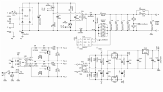
I found a control circuit which consists of  several TL072D  in which I could not understand its operating theory, so ask you for technology supports.

there are parts of understands for me and some queries below:

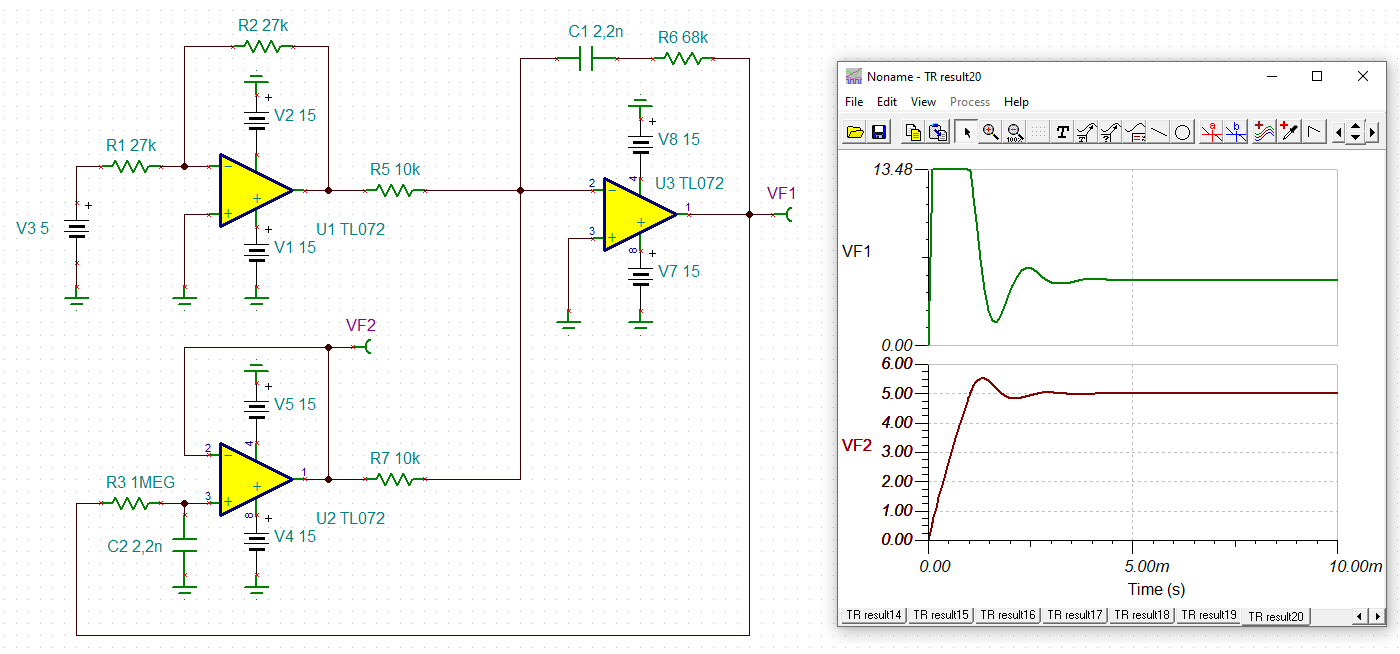
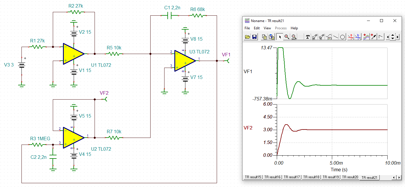
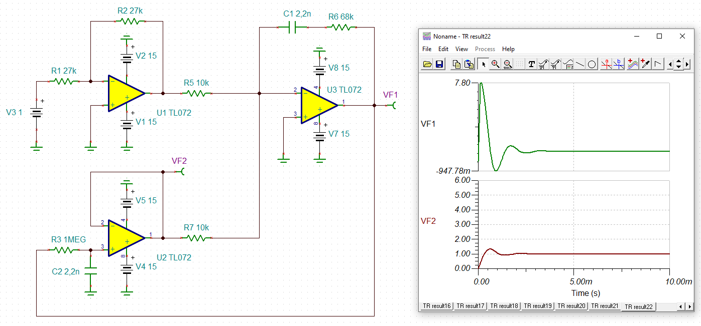
1. About the required voltage and U-feedback. The R18/ R21 are a summing networks, that and IC5A will compose a inverting summer with PI controller. I confused how the u-feedback can be synchronously changed by adjusting  the P1.Should the u-feedback be follow or equal to the p1 voltage value ( means the voltage of u-feedback equal to voltage of P1 adjusted) ?   Might the IC4A, IC4B and IC5A be merged an error amplifier ?

2. About the required current and I-feedback. The R30 and R29 are a summing networks, that and IC9A will compose a inverting summer with PI controller. Should the voltage of I-feedback can follow or equal to the voltage of P2 adjusted ? 

3. About the PWM_duty_set. Should the voltage of  PWM_duty  will be changed by P1 adjusted and P2 adjusted ?

the attachment is circuit diagram for your reference.

  • Hi Meng,

    don't overlook C25 and C29. IC5A and IC9A are integrators. The output voltage of an integrator remains constant, when no current is flowing into the integrating cap. This is the case when the input currents through the 10k resistors (R18/R21 and R29/R30) exactly cancel.

    Kai

  • Hello Meng,

    The voltage where R18,R21 cancels is IC4A = -IC4B ; the sum is zero volts ( IC4A + IC4B = 0V)

    The voltage where R29,R30 cancels is IC6B = -IC7B ; the sum is zero volts ( IC6B + IC7B = 0V)

  • Hi Kai,

    Thanks for your assistance !

    I did a circuit simulation with Tina such as the attachment.

    As may be seen from the diagram, the IC5A output is 3.83v , that shows the input sum (R18/R21 [ VM7+VM4=-10.509V] R30/R29[ VM13+VM20=2.42v] ) don't cancels. I have no idea where the problem are ?

  • Hi Ron, 

    Thanks for your explains in details, The see the circuit simulation from kai I sent.

    The IC4A don't equal to -IC4B and the IC6B don't equal to -IC7B , that make me confusing. I don't know what the problem is.

  • Hi Meng,

    Why is "U-Feedback" -11.08V? Is "U-Feedback" connected to anything at all? Looks like the feedback loop isn't closed.

    Kai

  • Hi Kai,

    The u-feedback should connect to a resistive divider of output voltage such as the attachment.

    I did not also find a negative feedback loop between IC4A and IC4B , So I confusesd how the u-feedback follow the P1 (required voltage). Might there be something wrong in the origional circuit diagram?

    Best,

    John 

  • Hi Meng,

    your simulation is just incomplete, as you didn't close the feedback loop. Add the regulator arround "TR1" to your simulation and connect the signals "U-Feedback" and "PWM". This will close the feedback loop and make the PI-controller properly work.

    Kai

  • Hi Kai,

    I did not find the SG3525 chip in Tina simulation software, Could you show the simulation circuit for the original design circuit in Tina or other simulation software ?  

    According to my understands the PWM-duty only is a variable DC voltage whose range is about 0.9V - 3.6V that is for chaging the pwm duty form 0 to 100%. The u feedback  should be a various dc voltage whose fuction is to control the output voltage through the divider resistors (R6+R7)/R7. If the u feedback can follow the voltage setting , there should be a negative feedback loop between IC4 - and pwm-duty or other circuit , however , there should consist a error amplifier among IC4A, IC4B , IC5A...., right ? but i could not find the negative feedback loop. 

  • Hi Meng,

    as I already said, you have to close the feedback loop. Here some examples:

    meng_tl072.TSC

    Kai