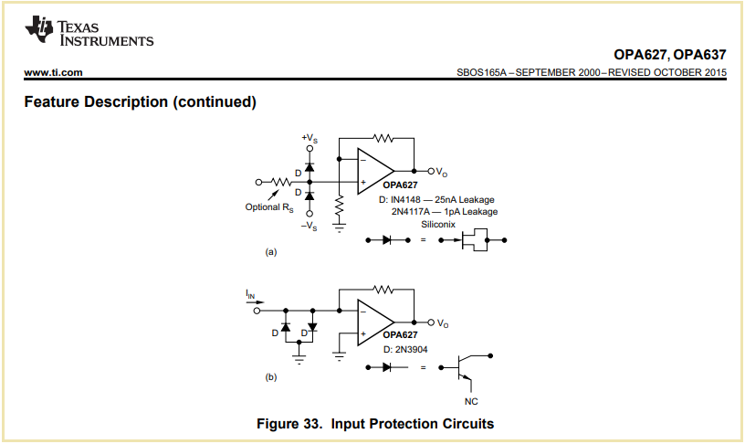
This thread has been locked.

If you have a related question, please click the "Ask a related question" button in the top right corner. The newly created question will be automatically linked to this question.

OPA145: ESD rating applicable when the device is powered ?

Part Number: OPA145
Other Parts Discussed in Thread: STRIKE, OPA627

OPA145 datasheet specifies that the device pins feature ESD ruggedness according to 2 kV Human body model.

1) Does this apply while the amplifier is powered up ?

2) Does this mean that the input protection diodes survive direct exposure to a 2 kV, 100 pF, 1.5 kOhm strike without additional components? Obviously the resulting current of more than 1 A for about 50 ns is way above the Absolute Maximum Rating of 10 mA.

Background: I have an application where the non-inverting input of the opa145 is directly exposed to a device interface and will be subjected to 61000-4 testing for ESD and EFT. *Of course*, I will provide additional protection, but it is a *HUGE difference* if this additional protection has to limit the 50-ns-transient current to something like several 100 mA or to a few mA.

Kind regards!

  • Hi Tobias,

    the recommended remedy is to use a diode clamp to the supply rails and to add a current limiting resistor between the diode clamp and the OPAmp input. The ESD is shunted into the decoupling cap then, so short traces from the diode clamp to the decoupling cap are necessary. Also, a ground plane is useful and mount the decoupling cap close to the supply voltage pins of OPAmp. Keep in mind that the decoupling cap can be charged up to a potential lying above the supply voltage. So if the voltage regulator cannot absorb reverse currents, add a TVS in parallel to the supply voltage decoupling cap.

    When it comes to ESD, more has to be considered: Never allow ESD running across the whole PCB. So it's wise to shunt ESD right at the entry point to the metallic enclosure. This is done by mounting a 10nF/1kV cap from the grounding point of decoupling cap to the metal enclosure.

    An even better way is to have an own decoupling cap for the diode clamp (and the ESD!) right at the signal entry point and to have the OPAmp a bit distanced apart. Move the 10nF/1kV cap to the decoupling cap of diode clamp. Have a "dirty area" for all these ESD currents (and eventual added low pass filtering) and mount the OPAmp in a certain "safety" distance.

    Make no mistake, the ESD ratings of OPAmps only give some minor protection during the handling and assembling, but they do not provide sufficient protection against industrial ESD events, covered by the 61000-4. So additional protection measures are obligatory, when the pins of OPAmp have contact to the rough industrial environments.

    Kai

  • Dear Kai, thanks for taking the time it took to write this reply. Unfortunately, it does not answer either of the two questions. I did not ask about conventional ESD countermeasures, but about the details of the stated HBM specification for the OPA145.

    I am well aware of how to safely handle ESD. However, sometimes these conventional countermeasures cannot be used such as in this case. In particular, I cannot use rail clamps, due to leakage requirements, so I have to rely on series impedance to limit ESD current. Back to my question -> For the typically very short durations of ESD, can the *internal* ESD diodes handle more than 10 mA as is suggested in the datasheet due to the HBM ESD rating?

  • Hi Tobias,

    yes, of course do they handle more than 10mA, but only for some nsec.

    A current limting resistor can be used against high ESD. But keep in mind that ESD can arc over across the resistor, not only externally but also internally across the windings of helix. So you would need to place several resistors in series and/or use so called carbon composition resistors which are specialized for handling ESD. Carbon composition resistors do not have a helix or windings but are made of a solid carbon film.

    What protection measures are you planning? Can you show a schematic?

    Kai

  • No schematic, but a hopefully detailed description: The device interface has shunt diodes to a guard ring, so it is not entirely without parallel protection. However, for ESD strikes, as a result of the large current in the shunt diodes, the interface node voltage still would rise to ~50 V  for 8kV 61000-4-2 strikes which is 35 V beyond the rails. If I add 1 kOhm series resistance impedance in front of the opamp, the input current would be around 35 mA-peak for the duration of the strike (~50-100 ns). Some people say, this is enough to cause latch-up, others say: It is safe, because according to datasheet section 6.2. (HBM ruggedness), the ESD diodes can even handle 1 A for the duration of an ESD strike.

    So now I am here hoping for a reliable answer from TI Slight smile

  • Hi Tobias,

    if the current spike is really lasting as short as an ESD event, then the 1k resistor might do. But if it's longer lasting the current should be limited to 10mA. Let's see what TI is saying to this.

    35mA times 100ns makes the voltage of a 100nF decoupling cap rise by U = Q/C = 35mA x 100ns / 100nF = 35mV. So this should not result in a relevant reverse current issue.

    There's another remedy you could use, a filter cap to signal ground behind the 1k resistor. A 100nF could absorb the ESD resulting in a voltage increase of 35mV. Even a smaller cap could be very helpful.

    Kai 

  • The only node that can be used realistically for shunting is the guard node, and even then, not for any component. Leakage should be below 1 pA at room temperature at max. 1 mV difference between the guard and interface node. Many diodes at 1 mV bias have already more than 1 pA current. Anyway, capacitors/diodes to VDD/VSS/GND all produce too much leakage.

  • Yes, it's hard to find components with sub-pA leakage current.

    Can you increase the 1k resistor?

    Kai

  • Rather not as it would deteriorate the input noise. Thanks anyway! However, I didn't come here for ways to bring input current to below 10 mA, but asking whether more than 10 mA are fine during an ESD strike - while the part is powered.

  • Hi Tobias,

    Regarding your questions:

    OPA145 datasheet specifies that the device pins feature ESD ruggedness according to 2 kV Human body model.

    1) Does this apply while the amplifier is powered up ?

    No. The 2kV HBM applies to the unpowered, out-of-circuit handling and assembly environments.

    2) Does this mean that the input protection diodes survive direct exposure to a 2 kV, 100 pF, 1.5 kOhm strike without additional components? Obviously the resulting current of more than 1 A for about 50 ns is way above the Absolute Maximum Rating of 10 mA.

    The OPA145 ESD protection circuitry HBM rating conforms to the established 100 pF, 1.5 kOhm, 7500 nH series model established to mimic an out-of-circuit handling and assembly ESD condition. The peak current can be very high, in the ampere range for that condition but as noted the duration is in the tens of nanoseconds. The ESD diodes might become involved in an in-circuit electrical overstress (EOS) condition where they could be turned on. In which case, that might be a DC condition and the OPA145 ESD diode can handle a continuous current up to 10 mA.

     Regards, Thomas

    Precision Amplifiers Applications Engineering

  • Thanks Thomas for the information!

    There is only one sentence that is a bit unclear to me, but seems very important for my understanding:

    In which case, that might be a DC condition and the OPA145 ESD diode can handle a continuous current up to 10 mA.

    Could you elaborate a bit please? Many sources on the internet agree that 10 mA is a typical absolute max figure for the DC overstress. But I am not asking about in-circuit DC overstress behavior, I am asking about in-circuit 61000-4-2  ESD compliance, which is a tightly controlled test. The time profile is very similar to the HBM ESD test, but the main difference is that the device would be powered. TI's own document here (https://www.ti.com/lit/an/slya014a/slya014a.pdf) suggests that parasitic SCR has a transition frequency of ~1MHz in CMOS ICs. I imagine that analog ICs it could be even slower, as analog circuits are not so tight. So what do you consider a DC overstress ? 1µs ? 10 ns ?

    Would the circuit, when powered, survive a 50 ns event that pushes ~50 mA through the input ESD diodes or would latchup occur?

  • Hi Tobias,

    I know this doesn't answer your question. But, in any case, I would take the 2N4117 and build a diode clamp, as shown in the datasheet of OPA627:

    If only 1k series resistor is allowed, I would split it into a 510R resistor in front of the diode clamp, to limit the current through the FET and a second 510R resistor between the diode clamp and the input of OPAmp.

    The purpose of this diode clamp is not only to protect the OPAmp against your limited ESD, but also to provide protection against all those scenarios you are not thinking of. Think about applying an input voltage during power down, applying non limited ESD and all sorts of incorrect connections.

    Kai

  • Hi Tobias,

    It is evident that the test conditions, pulse speed and current levels developed at a particular kV level for 61000-4-2 and HBM ESD testing are quite different from each other. One paper I found comparing these two ESD tests indicates that the peak current in 61000-4-2 test can result in >5x current than the HBM test. Our Precision Amplifier ESD cells are rated for HBM and CDM ESD events, and not the 61000-4-2 event.

    We do not test to 61000-4-2 when we are doing the initial product ESD verification t and don't have information how it would respond to it.

    Regards, Thomas

    Precision Amplifiers Applications Engineering