This thread has been locked.

If you have a related question, please click the "Ask a related question" button in the top right corner. The newly created question will be automatically linked to this question.

JFE150: Ultra-Low Noise Piezoelectric Amplifier TINA-TI Reference Circuit

Part Number: JFE150
Other Parts Discussed in Thread: TINA-TI, , OPA202

Hi !

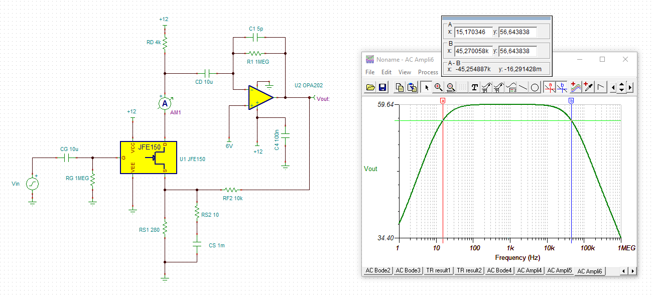
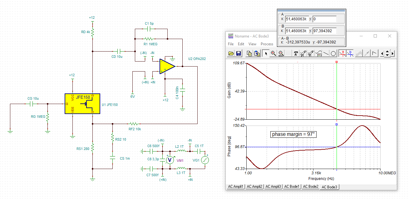
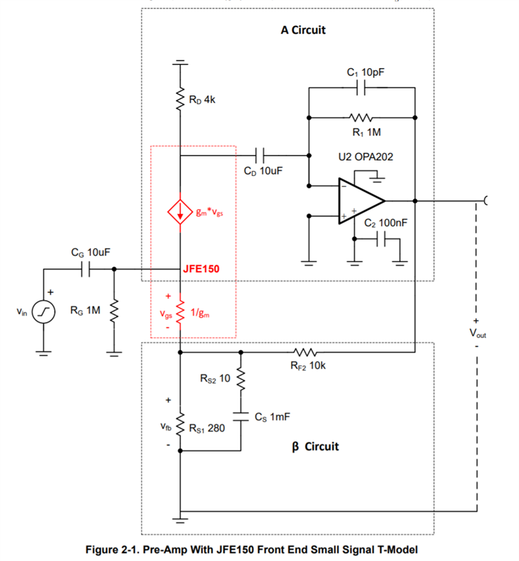
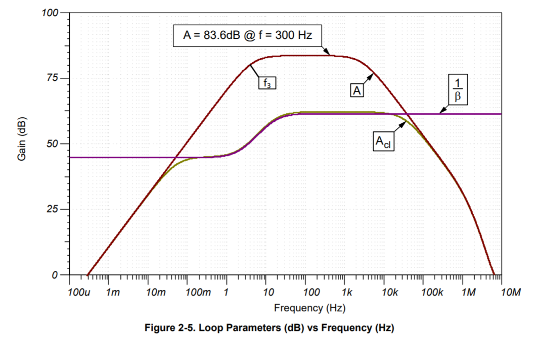
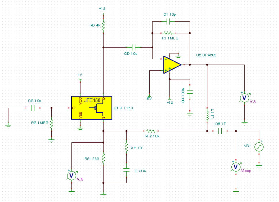
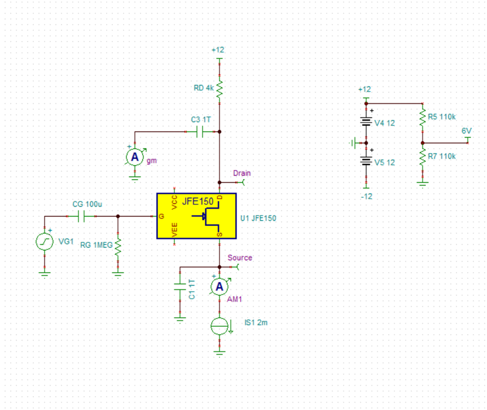
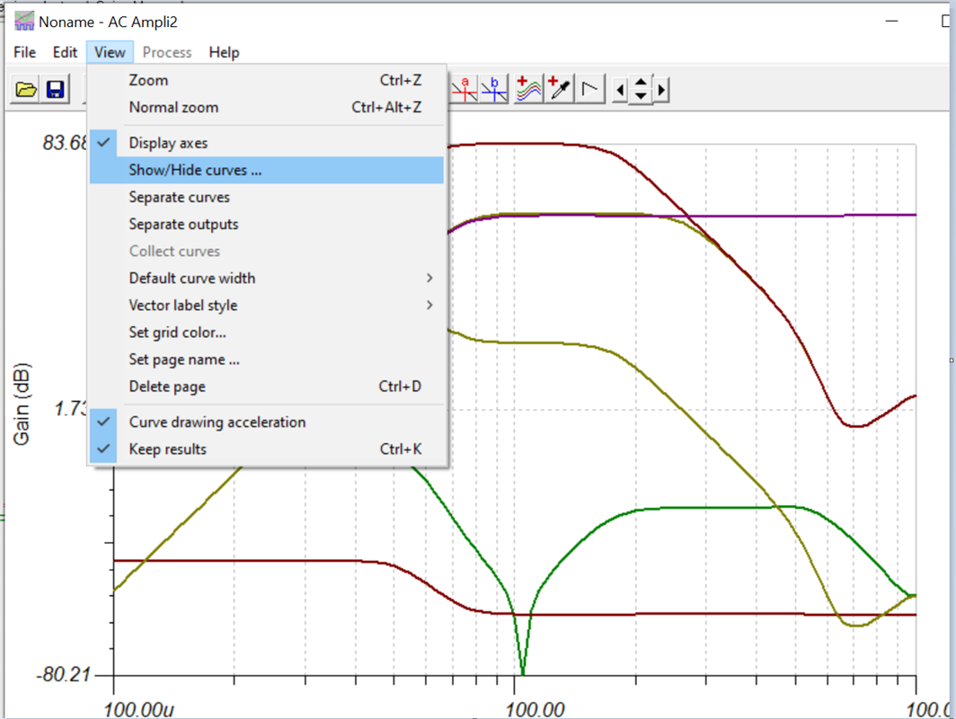
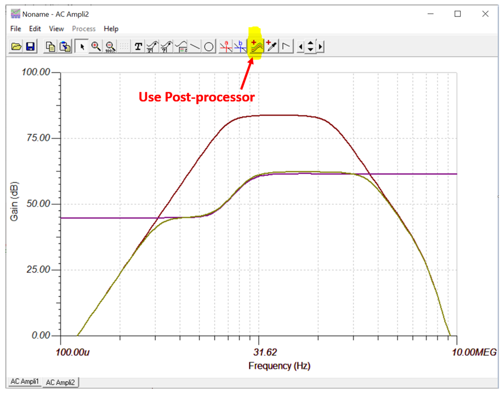
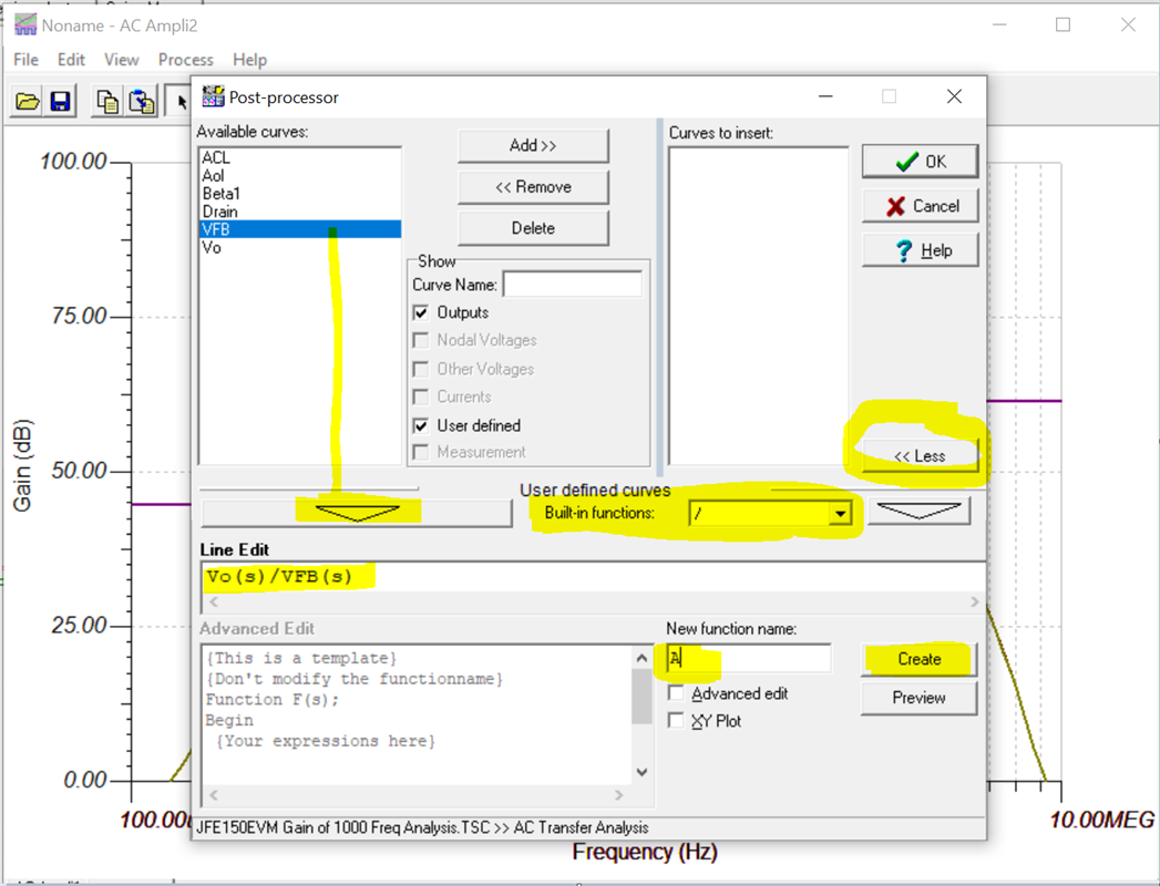
I'm using JFE150 Ultra-Low Noise Piezoelectric Amplifier TINA-TI Reference Circuit(SLPM352.ZIP ).

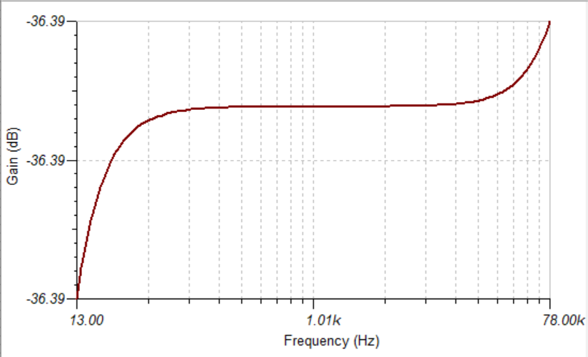
The frequency response of this circuit is about 24kHz@-3dB.

What determines this frequency(24kHz) in the circuit?

Best Regards,

  • Hi Daisuke,

    the frequency response can be extended a bit by decreasing C1:

    daisuke_jfe150.TSC

    daisuke_jfe150_1.TSC

    Kai

  • Hello,

    Great question! I have written a detailed app note that goes into all the details of this circuit including the -3dB point in the link below.  

    https://www.ti.com/lit/an/slpa018/slpa018.pdf?ts=1644457125558&ref_url=https%253A%252F%252Fwww.ti.com%252Fproduct%252FJFE150

    The circuit can be analyzed in the Hybrid-T model and the A-Circuit and Beta circuit are shown below. 

    The feedforward gain A is a function of the OPA202 bandwidth. The upper –3 dB point of Acl occurs when A and 1/β meet. In the app note I teach how to perform this analysis in Tina-Ti. 

    Let me know if I can help further. 

    Best Regards,

    Chris Featherstone

  • Hi Chris,

    Thank you for the application note. This is what I wanted to know.

    But I'm not good at TINA-TI...

    Could you tell me the following?

    1. How can I display Figure 2-2(gm vs frequency) of the app note in TINA-TI?

    2. I tried to display Figure 2-5 of the app note.
    I displayed A and β as follows. Is there an easier way?

            In the attached circuit,

    • Analysis  ->  AC Analysis  ->  AC Transfer Characteristic
    • Display A and Beta using the post processor on the Bode diagram of the calculation result.
      • A = V_A(s) / V_fb
      • 1/Beta =  Vloop / V_fb

    Best regards,

    Daisuke

  • Hello Daisuke,

    In order to simulate the gm of the JFE150 device, a different circuit was used as shown below. At frequency the 1TF capacitors C3 and C1 become a short. By placing a meter at the drain gm can be measured at frequency. The capacitor C1 is placed at the source in order to make this node AC gnd, at frequency while still allowing for a DC bias for the JFE150. The gm in this case was measured under the condition of the DC IDS bias current equal to 2mA using the constant DC current source IS1. I have attached this simulation below. Note that the result you will see here vs my application report are slightly different. This is because the model we provide is the latest model that is more accurate. I used a prior model for my application note. 

    JFE150 gm Simulation.TSC 

    In order to display the parameters A, Beta 1 and ACL in Figure 2-5 you have to use post parameters feature after running the AC frequency analysis. 

    Remove the curves you don't want to view

    Click More button to expand window. Select available curves and drop them into the Line Edit. Name the function under the New function name section and click create. I have attached my simulation below that contains the curves created by the functions in my app note. 

    For more in depth details on using Tina TI for stability analysis we have a video series that will walk you through the steps. This is the series I used in order to create the details within the app note regarding stability and Tina TI.

    JFE150EVM Gain of 1000 Freq Analysis.TSC

    https://training.ti.com/ti-precision-labs-op-amps

    Best Regards,

    Chris Featherstone

  • Hello Chris,

    Thank you for the detailed explanation and the simulation model.

    I understood well.

    You are perfect!

    Best Regards,

    Daisuke