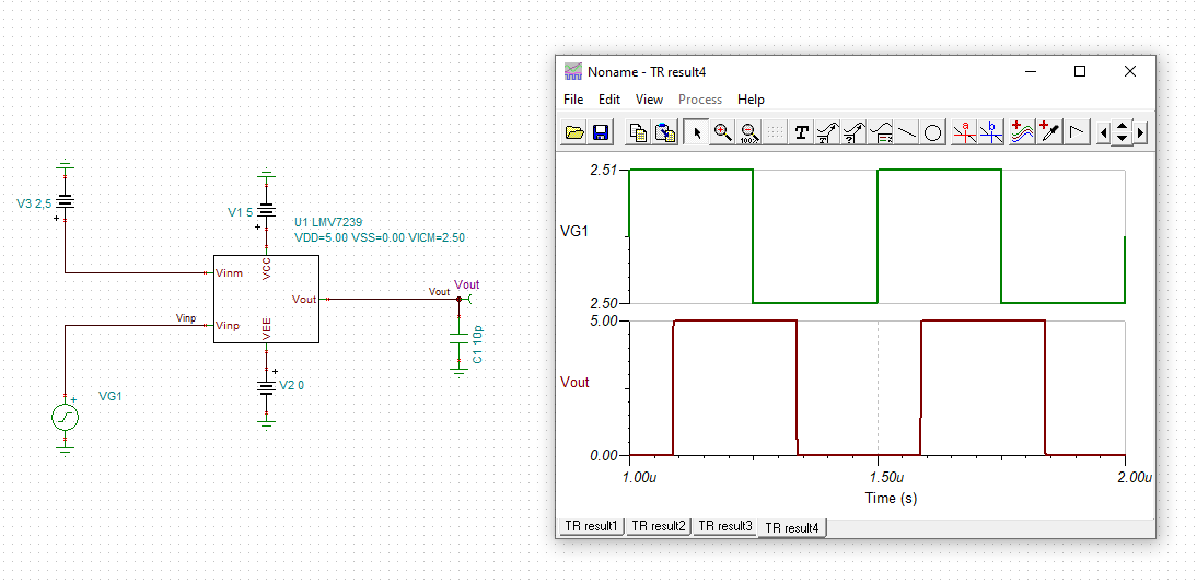
Hi, team
my customer want to use LMV7239 in 2MHz application, output cap will <10pf, in the datasheet 7239 propagation delay is 75ns.
we think it could work, and could you help to double confirm our scenario? thanks.
BR
Chi
This thread has been locked.
If you have a related question, please click the "Ask a related question" button in the top right corner. The newly created question will be automatically linked to this question.
Hi, team
my customer want to use LMV7239 in 2MHz application, output cap will <10pf, in the datasheet 7239 propagation delay is 75ns.
we think it could work, and could you help to double confirm our scenario? thanks.
BR
Chi
Hi Chi,
could work under ideal conditions:
But the concrete performance depends on many other factors like supply voltage, common mode input voltage, supply noise, signal noise, etc. Eventually, adding hysteresis might be necessary.
Can you show a schematic?
Kai
Hello Kai,
Thank you for your quick help on this thread :)
Hello Chi,
Thank you for your question. I would like a little more information about the details of your use case.
Can you provide a schematic and the voltage levels of the input signal? This way I can better understand the design parameters that Kai mentioned.
supply voltage, common mode input voltage, supply noise, signal noise, etc
Best Regards,
Joe
Applications Engineer
Linear Amplifiers Business Unit | Comparators Product Line (CMPS)
All information in this correspondence and in any related correspondence is provided “as is” and “with all faults”, and is subject to TI’s Important Notice (http://www.ti.com/corp/docs/legal/important-notice.shtml)
Hi, Kai and Joe
here is more inputs, supply voltage is 3.3V, noise is 20mV. input signal is single-end +-1.5V 2MHz, bias is 300mV. output is 3.3V LVCOMS
BR,
Chi
Hi Chi,
Thank you for providing more information. From what I gather, your input signal will swing from -1.2V to +1.8V for a total 3V swing? I am not sure what you mean by the bias is 300mV.
Assuming that your 20 MHz input signal is close to 50% duty cycle, you can AC couple the input (IN+) and set the common mode voltage with a resistive divider.
Best Regards,
Joe
Applications Engineer
Linear Amplifiers Business Unit | Comparators Product Line (CMPS)
All information in this correspondence and in any related correspondence is provided “as is” and “with all faults”, and is subject to TI’s Important Notice (http://www.ti.com/corp/docs/legal/important-notice.shtml)
Hi Chi,
Thank you for providing that info.
AC coupling the input to IN+ should work for your application so long as the input signal is 50% duty cycle. Just to confirm, is this the case?
Best Regards,
Joe
Applications Engineer
Linear Amplifiers Business Unit | Comparators Product Line (CMPS)
All information in this correspondence and in any related correspondence is provided “as is” and “with all faults”, and is subject to TI’s Important Notice (http://www.ti.com/corp/docs/legal/important-notice.shtml)
Hi, Joe
yes, it is the case using AC coupling in IN+ and duty cycle is 50%.
in my understanding, IN+ have +1.5V to -1.5V voltage range, it will be over our supply range 3.3V, it still will work? or using resistor divider in IN+ to decrease the -1.5V in IN+
BR
Chi
Hi Chi,
Your application will work if you AC couple the inputs and set your bias voltage of the resistive network to 1.5V.
This would result in your input swinging from 0V to 3.0V.
After doing this, the threshold has to be increased to 1.5V or 1.8V if you would like that 300mV bias you mentioned.
Please let me know if you need further explanation or clarification.
Best Regards,
Joe
Applications Engineer
Linear Amplifiers Business Unit | Comparators Product Line (CMPS)
All information in this correspondence and in any related correspondence is provided “as is” and “with all faults”, and is subject to TI’s Important Notice (http://www.ti.com/corp/docs/legal/important-notice.shtml)
Hello Kai,
From the image that Chi provided, the input looks to be a square wave.
Chi,
Please reach out if you need further explanation on this.
Best Regards,
Joe
Applications Engineer
Linear Amplifiers Business Unit | Comparators Product Line (CMPS)
All information in this correspondence and in any related correspondence is provided “as is” and “with all faults”, and is subject to TI’s Important Notice (http://www.ti.com/corp/docs/legal/important-notice.shtml)
Hi Chi,
if the signal is a square wave, then even a simple diode level shifter could do, sometimes:
The two diodes do the main level shifting. R3 is the assumed source impedance. R1 and R2 limit the current through the diodes and into the source. R1 helps to make the shifted signal better fall into the desired 0...+3.3V window. R4 helps to minder the spike current through the 10pF load capacitance in the moment when the source signal toggles and this without affecting the level shifting.
Kai
Hi, Joe and Kai
Thanks a lot for your test result and support, I will update to my customer and any question will keep you posted, thanks
BR
Chi
Hi Chi,
Thank you for the update. I will wait for your feedback.
Best Regards,
Joe
Applications Engineer
Linear Amplifiers Business Unit | Comparators Product Line (CMPS)
All information in this correspondence and in any related correspondence is provided “as is” and “with all faults”, and is subject to TI’s Important Notice (http://www.ti.com/corp/docs/legal/important-notice.shtml)
Chi
Sorry for the follow up on this. We just don't like things to go too long without a response.
Are you still waiting for feedback or can we close this post as resolved?
Chuck
Hi, Chuck
customer has accepted this solution, and didn't have any more question so far.
Thanks a lot for your help
BR
Chi