This thread has been locked.

If you have a related question, please click the "Ask a related question" button in the top right corner. The newly created question will be automatically linked to this question.

VCVS

Other Parts Discussed in Thread: TINA-TI

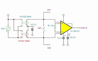
I've seen a voltage controlled switch used in TINA-TI, to switch between two inputs to an INA, presumably in order to facilitate analysis of VCM vs Vout associated with the inverting and non-inverting inputs connected to a single source. I looked around to see if I could find a functional diagram which explains just how the source is switched between the two INA inputs.

Can someone point me to an article or source which explains how this switch is used, in terms of how often it switches, etc., basically how it works. I get the impression that in this context, the switch facilitates analysis of the behavior of the common mode voltage (CMVin) in relation to the area of linear operation of the INA by switching between the inverting and non-inverting inputs.

I'm including a Tina-TI screen of the circuit.
Thanks

Bob Edwards

  • Hi Bob,

    this is no switch, it's a "Voltage Controlled Voltage Source", VCVS. The reason the VCVS is used here, is very simple: TINA-TI allows only one voltage source, when performing a "DC transfer characteristic analysis". Remember that we wanted to simulate a differential signal sitting on a common mode voltage of 3.3V. For this sort of simulation two reverse polarized voltage sources would be needed, which TINA-TI cannot handle. So I took only one voltage source (VG1) and generated from that two reverse polarized voltage sources by the help of mentioned "Voltage Controlled Voltage Sources". That's all Relaxed

    Kai

  • Thank you Kai. You had me worried ;-)