This thread has been locked.

If you have a related question, please click the "Ask a related question" button in the top right corner. The newly created question will be automatically linked to this question.

INA240: optimal placing

Part Number: INA240

Hi,

I'm unsure what would be the optimal solution to place a INA240 for lowest noise for the current measurement.

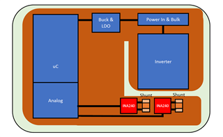
I'm using two INA240 for a motor control application and would like to get the optimal performance out of it. I'm using one solid GND plane for the whole board and separte the analog and digital signals by spatial serparation. Now I would like to know, where I should place the INA240 on the board, since I already saw different designs with different variants, where the INA240 is close to the shunts or where it is close to the ADC. 

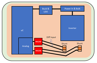
From my point of view it makes the most sense to place the INA240 near the ADC and route the differential pairs to the shunts to remove the low frequency current influence from the Inverter on the GND pin of the INA240 and the OUT signal is only single-end and prone to noise. From a EMI point of view, it would probably be better to have the differential pair close to the shunts, to remove the antenna length for the HF PWM signals.

1.) Directly placed at the shunts and loop the output back over the board to the ADC

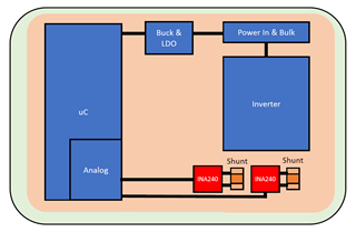
2.) Placed the INA240 close to the ADC input and loop the differential pair to the shunts

So my questions are:

1.) What is the best placing solution for lowest noise of the INA240?

2.) Is the return current for the IN+ the IN- signal or the GND? For me it looks like it is the GND, since a OPAMP is integrated.

3.) Is a LPF recommended on the OUT pin of the INA240 to reduce noise and how much larger should be the cut-off frequency than the sampling frequency? 20dB?

Kind Regards,

Sebastian

  • Hi Sebastian,

    in order to keep the common mode rejection of INA240 high, the INA240 should sit closest to the shunt. If you have the shunt distanced from the INA240, on the other hand, the two connections between the shunt and the INA240 inputs would see different stray capacitances. This would degrade the balance of both inputs and ruin the awesome common mode rejection.

    Also, with long connections between the shunt and the INA240 inputs EMI hitting these connections could inject different amounts of interference into the both input lines and by this convert common mode EMI into differential EMI which the INA240 could no longer suppress by the help of its huge common mode rejection.

    So the best place for the INA240 is closest to the shunt.

    If you cannot have enough distance between the INA240 and the motor control some shielding of INA240 can help. Also, avoid running PWM signals like motor currents, etc. over the common solid ground plane. Even avoid capacitive stray coupling of these signals into the solid ground plane. It's good to have a common solid ground plane for the INA240 and the ADC section. But don't have the motor control currents running over this ground plane. PWM applications with large currents and steep edges is one of the cases where a common solid ground plane for all the electronics might not be the best choice.

    A low pass filter directly at the output of INA240 is a good idea, as this would shunt EMI through the filtering cap to signal ground and no longer into the output of INA240.

    Eventually, you will need more than one attempt to get an optimum layout. I would think about splitting the ground plane into a power ground plane and an analog/digital ground plane and use shielding of both sections, if there are still issues. Shield the analog/digital section and connect this shield to the analog/digital ground plane and shield the power section and connect this shield to the power ground plane. Find an optimum place where you connect these two ground planes together.

    With a bit luck no shielding is necessary, or only shielding of the analog/digital section.

    Kai

  • Hi Kai,

    Thanks for your detailed answere. 

    Good to know to place the INA240 close to the shunts, I always placed it a bit away to reduce the effect of the stray currents, but never tought about the CMRR could decrease.

    The GND split is a topic I had many discussions with many engineers and there seems to be exceptions where it is a good idea to split it, especially high LF currents like in this application. But many engineers also told me, that when the signals are enough spatially separeted, there is nearly no coupling into the ADC section and a solid GND plane (also for the inverter currents) is the optimum design. Also all the HF currents are following the tracks and are shunted over the bypass caps. It would be extremly interesting to compare a GND split with a solid GND plane for exactly the same setup. 

    So what I could do is to split the GND plane something like this:

    Here the GND plane is still solid except the inverter power stage has a separated return path in the GND layer and LF currents cannot couple directly into the INA240 measurements The GND is then connected at the Bulk Caps. There will be no digital signals over the analog GND plane partition. What do you mean by shield the ground plane?

    What I further saw in the datasheet is, that there is an absolut maximum voltage rating for the INA240 of -6VDC for common mode signals, so if through parasitic inductance (GND split) and the high currents somehow the two GND has a potential difference of less than -6VDC, the INA240 is gone. But I think that might be not a problem at 40-50A and a huge (splitted) GND plane for the return currents as depicted above.

    Kind Regards,

    Sebastian

  • Hi Sebastian,

    I'm also a fan of a common solid ground plane. And I would first try to not split the ground plane. But I have learned that there are certain situations where a split of ground plane might be advantageous.

    Voltage drops of LF currents can be minmized by "thickening" the copper of ground plane, either by chosing 70µm copper (or more) instead of 35µm. Or by mounting 0R bridges in parallel with the ground plane. Another option is to use more than one ground plane in the multilayer board.

    Voltage drops of HF currents can be minimized by routing the currents very close on top of the underlaying ground plane, as you already said. The proximity effect makes that the ground return current follows the path of least inductance within the ground plane, which is exactly underneath the HF current. The problem is that the proximity effect becomes way less strong when the currents are no longer flowing on the printed circuit board, or by other words, close to the ground plane but are forced to run through components far away from the printed circuit board and the undelaying ground plane, as it can seen with power circuits. Then, the ground return currents can spreaden over the whole ground plane.

    What I further saw in the datasheet is, that there is an absolut maximum voltage rating for the INA240 of -6VDC for common mode signals, so if through parasitic inductance (GND split) and the high currents somehow the two GND has a potential difference of less than -6VDC, the INA240 is gone.

    Aggreed! This issue would demand to use a common, unsplitted solid ground plane and by this minimizing unwanted stray inductances.

    I think it cannot be said what is better without thorough testings.

    What do you mean by shield the ground plane?

    I wanted to say that when coming with an EMI current too close to a ground plane, unwanted compensating currents can flow within the ground plane which can cause unwanted voltage drops within the ground plane.

    To your picture: You could try to move the shunt / INA240 combination a bit closer to the ADC.

    Kai 


  • Hello all,

    I agree with Kai about the Rshunt should be closest to the INA240 and about having an output filter.

    As far as the GND split vs. solid GND plane what was said about the split GND potentially harming the INA240 is a concern. 

    Regards,

    Castrense