This thread has been locked.

If you have a related question, please click the "Ask a related question" button in the top right corner. The newly created question will be automatically linked to this question.

INA226: INA226 fails frequently

Part Number: INA226

Hi Sir Or madam,

INA226 on our board has been failing frequently recently.  

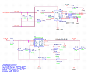
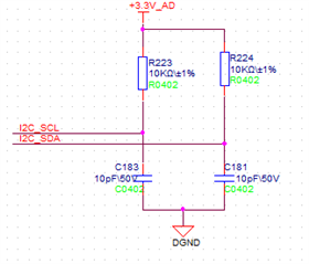
Phenomenon: INA226 collects the voltage and current of the load, transmits it to FPGA through I2C, and then transmits it to the upper computer through serial port. However, the voltage and current monitoring is 0 frequently recently (the load voltage is 24V;  Load current is dynamic, 200-500mA dynamic change)  ,I tested the power supply voltage of the chip and the impedance of each PIN to the ground on the board. The voltage of the 6th PIN VS of the chip was 0.85V and the impedance to the ground was 114 Ω,After the replacement of INA226 chip, the voltage and current monitoring on the upper computer are normal, but the problem has not been figured out.

Schematic diagram is as follows:

  • Hi Ian,

    is there a difference between the potentials "DGND" and "DGND_COOL"?

    Kai

    • There is no difference here, but the ground is separated in layout

  • Hi Ian,

    separation can mean additional inductance between the two grounds. And inductance can mean inductive kick backs and undervoltage damage of the inputs of INA226.

    Kai

  • Hello Iam

    Thanks for coming to the forum. 

    I agree with Kai. All grounds with the INA226 should be the same at the very least. Other devices connected to the same SCL and SDA bus lines should also have the same ground. Ground loops can easily damage IC by causing the input VCM of INA226 to go below -0.3V with respect to INA226 GND pin.

    So at the least you need the make the grounds of the following the same: INA226 GND pin, pull-down for address pins A0 and A1, decoupling capacitor C138, and pull down capacitors for SCA/SCL. 

    Or you could tie DGND and DGND_COOL with a low impedance cable.

    The following are symptoms of a damaged device:

    - high input bias current (measure voltage drop across R95 or R102) beyond datasheet specification limit

    - collapsing Vs voltage and/or increased supply current beyond datasheet specification limit

    - heated package

    - removing device from PCB and measuring low resistance from IN+/IN-/A0/A1/SDA/SCL  pins to device ground pin

    Sincerely,

    Peter

  • OK ,thanks a lot !