This thread has been locked.

If you have a related question, please click the "Ask a related question" button in the top right corner. The newly created question will be automatically linked to this question.

INA181: Current sensing gain issue

Part Number: INA181

Hi,

I designed a three phase  BLDC motor controller having three shunt based current sensing circuits as shown below


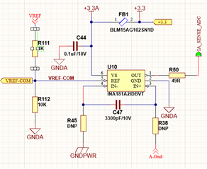
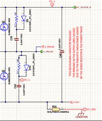
I set the zero current offset is at 1.65V. Here VREF is 3.3V. The input to the sensing circuit is taken from the shunt R36 ( image 2).

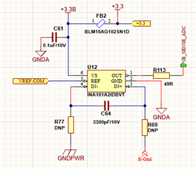
The same Reference voltage VREF-COM which is 1.65V is applied to all other sensing circuit.

I done the trace length match from sensing circuit to microcontroller and shunt to sensing circuit also. And the offset voltage is 1.6V for all sensor output at zero current input.

But while running motor the sensing circuit over all output gain is different . Two phases gave 6mV/A but one gave 10mV/A. 

Can some one please check and suggest some solution?

  • Hello valued engineer,

    I am looking this over and will respond shortly.

    Sincerely,

    Peter

  • Hello,

    You may want to check the abnormal device to see if it has been damaged from inductive kickback causing VCM to drop below -0.3V. You can tell if the device heats up more or is sinking excess current into pins.

    During the measurements is the output voltage (VOUT) saturating into supply rails? This could cause non linear behavior.

    sincerely,

    Peter

  • Hi,

    The sensor is not heats up even in high current . Based on the my design , it is capable measure up to 320A  for full scale. But I went to  maximum current up to 100A. Even low current also these are giving different gains.

  • Hi Joseph,

    the REF pins must be driven low ohmically, best with zero Ohm source impedance. A simple resistive voltage divider cannot serve this. You need an OPAmp to buffer the voltage divider as shown in figure 45 of datasheet.

    Kai

  • Hey Joseph,

    The motor current is not related to the potential heat up issue. The device can heat up if the the input common-mode voltage (VCM) rating has been violated (e.g., VCM < -0.3V). If VCM drops below -0.3V (with respect to INA181 GND pin), then this will forward bias the body diode of internal ESD protection circuits. It only take a several mA of current going into device pins to heat up ESD cell circuitry and cause thermal damage (either a short or an open). In the case there is a short, this can cause significant current to be sunk into device causing it to heat up further. So it is possible your device is experiencing an open and not heating up after being damaged.

    I also just noticed that the input resistors (R45 & R38) that connect shunt to INA181 inputs are not populated. Is this true? Are you running these tests with the IN+ and IN- floating? If so, this can be a serious problem.

    Assuming your input resistors are populated, you need to ensure that the input VCM for INA181 is not dropping below -0.3V due to inductive kickback or high impedance (inductance) between ground nodes GNDA, GNDPWR, A-GND, B-GND, C-GND, etc. All grounds always should be connected with low-impedance traces/cables. 

    You can use differential probes to measure voltage (on oscilloscope) between all ground nodes during motor operation and/or you could take the potentially damaged device and check for signs of damage. One way is to leave device on the PCB and populate input resistors (R45 & R38 with 100-Ohm resistors) and measure across these resistors during motor operation. If the input bias currents (IB = V_R45/100Ohm) are not within spec (<several uA), then there could be a short in the ESD cells circuits sinking excess current. Another method is to desolder the potential damaged device and to measure resistance between all pins and ground. Then also do this for a new, unused INA181 device that should not be broken. Compare the resistances between both device to see if there is an open or short.

    It is true that using a resistor divider to set REF voltage is not preferred solution because it creates additional gain and offset error, but it shouldn't be alone responsible for damaging device.

    Hope this helps. Please post back if you have more questions.

    Sincerely,

    Peter