This thread has been locked.

If you have a related question, please click the "Ask a related question" button in the top right corner. The newly created question will be automatically linked to this question.

LMH6703: SOT23-6 package

Part Number: LMH6703
Other Parts Discussed in Thread: OPA695, TINA-TI

Hi

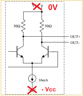
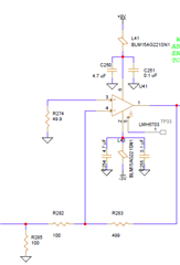
I need to drive the LMH6703 in the SOT-23-6 package from a CML output.

The CML gate will operate from negative supplies, so the output is internally terminated 50 ohms to GND

The CML output will preferably be DC coupled to the OPAMP circuit.

GAIN 5 or 6

My prime interest is rise time 0%-100%.  I don't mind slight overshoot.

The goal is a positive going pulse at the opamp output.  I can use the positive or the inverting output of the driving gate (the other output terminated to 50 ohms of course), so I can choose gain polarity of the opamp circuit.

Is it preferable to use the inverting or non-inverting configuration?  What will give me the faster rise time, and what will give me the faster slew rate?

Also - will the OPA695 give me better or worse performance for this design?

Thanks

Pinhas

  • Hi Pinhas,

    you mean something like this?

    Kai

  • correct.

    with one of the outputs terminated in 50 ohms to GND 0V

    and the other feeding the LMH6703 circuit - in either inverting or non inverting configuration.

    I simulated in TINA-TI using a current sink on 50 ohms to GND instead of the gate - and it looks good into inverting.  might be good on both.

    But apart from anything else - I think the model in TINA is the SOIC version of the 6703.....

    thanks

  • Hello Pinhas,

    Good questions!  Both the LMH6703 & OPA695 are current feedback amplifiers, so their architecture allows for reasonably high slew rates (~4300V).  Depending on your 

    For the OPA695, examine Figures 5 & 6, 25, 36-39 for additional information on rise time & small-signal response based on noninverting vs. inverting configs.  The Electrical characteristics section provides a typical rise time of 1ns, with some room for variance at certain step-sizes, gains or applications.  

    In comparison, the LMH6703 has a rise time that is step-size-dependent, with a 2V step having a 0.5ns rise time while a 6V step has a 1.05ns rise time.  Considering your preferred gain and application, I would advise continuing to explore simulating your scenarios.  

    Does your comment on simulating in TINA confirm you found a working configuration?  Or are you still exploring what may be best?

    With regards to the TINA file being the SOIC version of the THS6703: the SOIC package contains two extra pins which are no connect (or N/C).  Since these pins add no functionality or capability to the SOIC variant, the SPICE model is sufficient regardless of whether you use TINA or PSPICE to simulate.  In general, if you do not see package-specific models for a part, the provided model is what you should use regardless of package type.  This would differ if one package had shutdown & the other did not, but the LMH6703 has a shutdown pin on both packages.  I confirmed by viewing the TINA model that shutdown is modelled for the LMH6703.

    Please let me know what else I can assist you with, or if you have a follow-up question.

    Best,

    Alec

  • Hi  Alec,

    Thanks for the response - I only got a mail about it now for some reason.  I am still exploring, but need to close a schmeatic for layout in the coming days, and I am trying to minimize risk

    1 - it says "Depending on your " and then starts a new paragraph - perhaps something was erased in error?

    2 - Regarding actual issues:

    Between the parts it seems the LMH6703 is likely better - and they are both pin compatible so no risk.  I have seen all those figures.  I also may drive the amp slightly into saturation - which renders those figures slightly less useful , and I hope the TINA simulation, and some work I have done with eval boards (with a different input) - gives some indication

    3 - I am well aware of the slightly different response between inverting and non-inverting, and indeed it is a tough call - seems the inverting will be a bit faster.  Assuming the simulation is accurate.  I expect I may need to tweak values a bit once built.

    This decision will be a point of no return once in layout - as these lines are layout sensitive so I don't want to risk "options"

    BUT - my question was regarding the DC coupled interface of ths input to the opamp block with the CML output - does it matter in terms of that? (to me seems not as long as I present a 50 ohm input load to the opamp curcuit - the series resistor and shunt resistor in parallel to present 50 ohms)

    4 - My issue with the packages is that according to the graph on page 12 of the LM<H6703 datasheet - there is a SIGNIFICANT difference in the optimum feedback resistor to be used between the SOT and SOIC package.  That's also what leads me to believe the model matches the SOIC...

    Thanks

    Pinhas

  • Hi Pinhas,

    my tipp is, don't rely all too much on the simulations. In this frequency range the layout plays a major role and it cannot be said with absolute certainty which RF is the best without performing any measurements. So you will have to do some prototyping first, before drawing the final layout and selecting the final components. 

    Can you show your TSC-file?

    Kai

  • Hello Pinhas,

    Were you able to make progress on layout/fabricating a board to measure performance?  Have you done any further simulations?  If you could share your simulation files (like TSC TINA-TI circuit file) and/or board layout, we could take a look and provide additional feedback.

    Best,

    Alec

  • clearly simulations are limited.

    and it sounds like both you and Alec agree that we can't really know which part is preferable without building it - the pinout is same anyway so I can test.

    regarding inverting vs. non-inverting, sound like no clear answer and that the simulation wont tell me for sure either (I didnt see much of a difference) - so I went with the inverting configuration.

    truth is - I think my primary question was regarding the direct DC couple interface to a CML output (GND as Vcc) - will that interface be fine or affect performance?

    hard to simulate that Slight smile

    I used a 8mA or 16mA current sink via 50 ohms from GND

  • Hello Pinhas,

    Regarding your primary question on the direct DC coupling of the amplifier to a CML: I do not see an issue with this design choice; since you are DC coupling with CML, you do not need to add the resistors necessary for an AC-coupled interface.  You are correct, it is a bit difficult to simulate this behavior.  I read through several documents on CML and did find this TI resource:https://www.ti.com/lit/an/scaa062/scaa062.pdf  It does not address our question here, but does contain some information about interfacing and CML.  

    Best,

    Alec

  • Alec,

    Thanks.  I am familiar with that document.

    And I appreciate the second opinion that is should work fine.