This thread has been locked.
If you have a related question, please click the "Ask a related question" button in the top right corner. The newly created question will be automatically linked to this question.
hi,
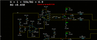
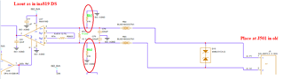
Need your help to understand and fix an unexpected results while using INA819 as amplifier with gain = 6.9
The op amp's power is single 5 volt dc and Gnd
It looks very simple, but does not work
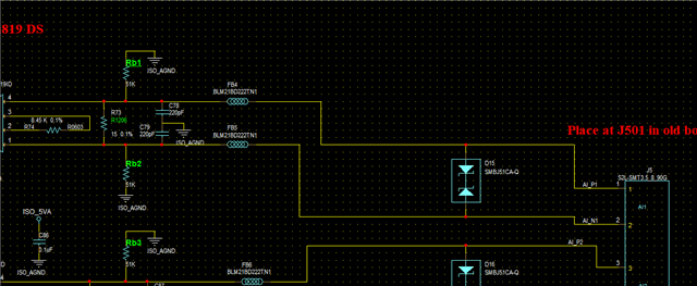
c81, c78 , c79 are not assembled.
Output is going to TI's ADS7828E Analog to Digital converter
The purpose of the design is to measure 4 to 24 mA dc current
The ref pin voltage is 2.5 volt driven by OPA191
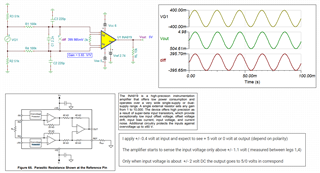
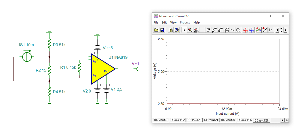
I apply +/- 0.4 volt at input and expect to see + 5 volt or 0 volt at output (depend on polarity)
The amplifier starts to sense the input voltage only above +/- 1.1 volt ( measured between legs 1,4)
Only when input voltage is about +/- 2 volt DC the output goes to 5/0 volts in correspond
I don't know how to solve it
please your advice
regards
Tsfania
Tsfania
Hi Tsfania,
There are several issues with the circuit.
1. If the differential input is ±0.4V with Vcm near ground, then you have to use bipolar supply voltage in configuration. If you are using 5Vdc as a single supply, then the input Vcm has to be configured above GND; the Vcm is optimized at the mid supply of 5Vdc or Vcm = 2.5Vdc. Please specify your Vcm mode voltage in the circuit.

Enclosed is the analog engineer's calculator, which it is used to check the linearity of differential input for given Vcm vs. Vout conditions.
https://www.ti.com/tool/ANALOG-ENGINEER-CALC
2. Rather than using ferrite beads to attenuate higher frequency (>10MHz), we may implement differential and common mode filters as shown at the input. The instrumentation amplifier(IA)'s input needs to be balanced and impedance should be matched. Otherwise, common mode noise may turn into differential signals, which are not part of the design interest. Ferrite beads does not precise impedance and its tolerance can vary up to +/-25%.
The differential capacitor should use NP0/CG0 type or you may use X2Y capacitor, which you should be able to purchase from mouser.com. However, you may place a ferrite bead at the power supply rail for the INA819 IA.

Regarding to the differential and common mode LPF filter calculation, please see the attached image below. You may find the reference in section 3.2.1 in the attached link below.

https://www.ti.com/lit/ug/sbou115c/sbou115c.pdf?ts=1646145708887
https://www.mouser.com/datasheet/2/611/x2y_filter_and_decoupling_capacitors-1771721.pdf
3. The IAs or Amplifiers do not like to drive capacitive load directly, which it will introduce pole within the feedback loop and create instability. Please remove the C81. You may place a low pass filter after INA819.
Enclosed is a schematic that is similar to what you have. Since I do not have all the design requirements, please consider this simulation as an example.
BTW, ADS7828E is SAR ADC, please check with our ADC supporting team. You have to implement Anti-aliasing + charge bucket filters in order to optimize the input filters. If system noise is a concern, you may require to perform noise analysis or calculation to optimize the setup.

If you have additional questions, please let us know.
Best,
Raymond
Hi Raymond,
Many thanks for your answer,
VCM is exactly 2.5 volt and connected to Ref input of the INA819
the capacitors are not assembled, so they not influence
the main problem is that the ina819 output do not respond to voltage at input until +/- 1.1 volt dc
ferrite will not block the output
noise is not issue yet, no gain is the problem
regards
Tsfania
Hi Tsfania,
The following Vcm vs. Vout is fairly close to your current IA setup. The circled orange figures are shown in min. and max. differential input should not go beyond ±0.35V on top of 2.5V. Your low end of input signal should be approx. 2.5 - 0.35 = 2.15V; and high end of input signal should be approx. 2.35V. So the input between 2.15V to 2.35V is your instrumentation amplifier's range, which Vout will keep a linear relationship with the input.

You mentioned that "the main problem is that the ina819 output do not respond to voltage at input until +/- 1.1 volt dc"
If I understood your statement correctly, your input is outside of the required input range of INA819 per the configuration, which it will not be linear. If INA819 responds to the input, it does not mean that Vout will be in a linear relationship.
If you applied +/-1.1V at the input of INA819, that means that your Vcm is not centered at 2.5Vdc. Please check with the Analog Engineer Calculator above and below Vin- and Vin+ in Max. and Min. requirements.
Based on your latest schematic, I do not see that the Vin+ and Vin- nodes have the common mode Vcm = 2.5Vdc. Can you show me what are Vcm at P1 and N1 at J5 node? It is some kind of sensor or wheatstone bridge.

Best,
Raymond
Hi Dear Kai, and Raymond,
Many thanks for your good advice.
My case have been solved by connecting negative power supply.
Now it works as expected
The problem starts with declaration in Data Sheet that INA819 works with Single PS.
There is no warning about limitation of Single PS .. way?
I must ask new question because of adding negative PS.
As i mainchain, the OPamp outputs are going to A2D with single 5 volt supply
Is it necessary to add protection at the A2D inputs against negative voltage that may occur ?
Best regards
Tsfania
Hi Tsfania,
Is it necessary to add protection at the A2D inputs against negative voltage that may occur ?

I am fairly sure that you will need to add anti-aliasing filter and kickback bucket filter in front of SAR ADC. You may use single supply rail op amp for the filter design and will clamp the output to GND, if INA819 may source negative output by accident and/or wrong sensor connections at input. Please consult these design requirements with ADC supporting team.
Best,
Raymond
Hi Tsfania,
The problem starts with declaration in Data Sheet that INA819 works with Single PS.
Yes, if you connect a load cell bridge or a similar circuit to the input of INA819 providing a common mode input voltage arround about middsupply. But in your case the common mode input voltage is zero and no single supplied instrumentation amplifier can handle such a situation.
There's another reason why you should not work without a negative supply voltage when your common mode input voltage is zero. You use an instrumentation amplifier because you hope to profit from the common mode rejection of instrumentation amplifier when your signal is superimposed by common mode noise. Right? But with a negative supply voltage of zero Volts and a common mode input signal of also zero Volts, there's no headroom at all for any common mode noise arriving at the input of INA819. So you will not profit from any common mode rejection.
Ok, you will need to add a negative supply voltage of -2V to make the INA819 to work at all and you will need to add some extra negative supply voltage to add some headroom for the rejection of common mode noise. So when you choose a negative supply voltage of -5V, e.g., the INA819 can abssorb a common mode noise of about +/-3V.
This leads me to my next question: Do you need this common mode rejection at all? Or can you connect the lower end of 15R shunt directly to signal ground? In this case a simple OPAmp circuit will do the trick. If not, if you need to have some common mode rejection and if you need to use an instrumenation amplifer, you will need to add an additional rectifier stage to eliminate any negative voltage from the signal going to the ADC.
Kai
Hi Dear Kai,
many thanks for your excellent support
I thought that the INA826 will solve it, but now i understand that even this will need negative PS.
i will add 5 volt negative supply
shcottky diode will clamp negative signal to GND, and protect the ADC
Thank you again and again
wish you the best
regards
Tsfania