This thread has been locked.

If you have a related question, please click the "Ask a related question" button in the top right corner. The newly created question will be automatically linked to this question.

INA125: Wheatstone bridge based pressure sensor output shows loading effect

Part Number: INA125
Other Parts Discussed in Thread: INA826, ADS7142, REF200, TINA-TI

Hi

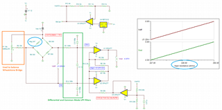
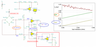
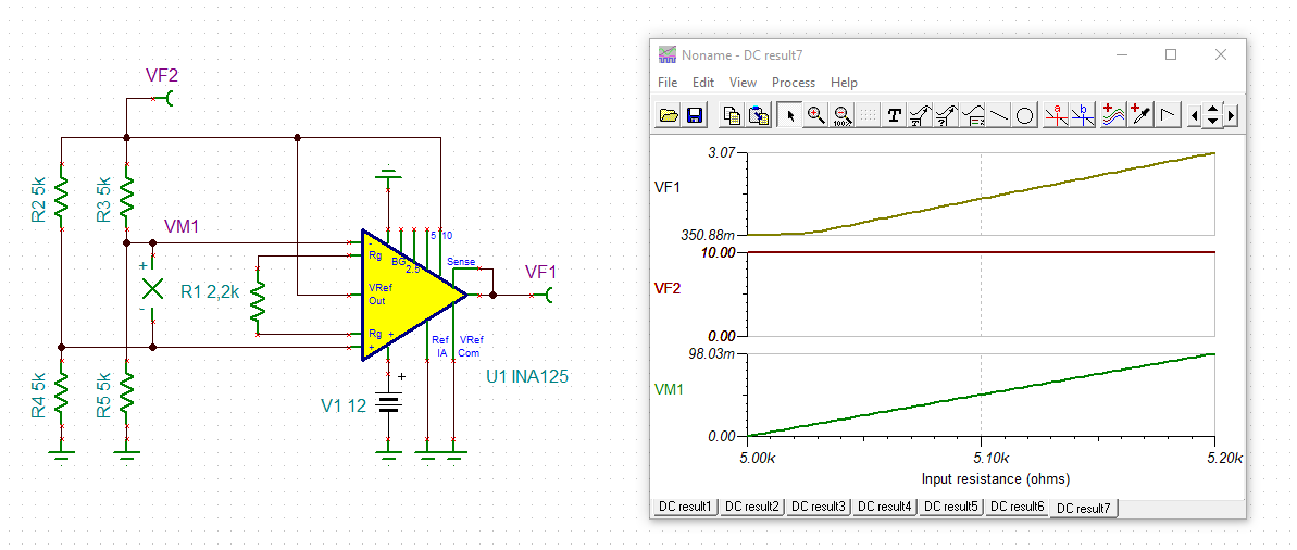
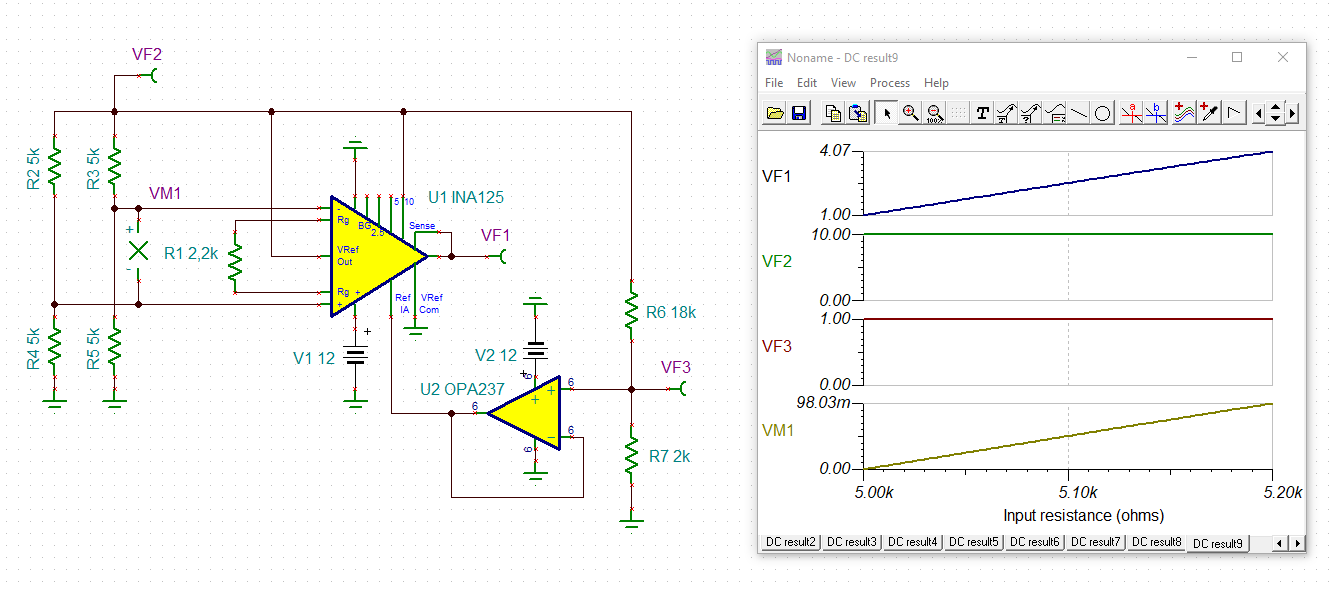
I'm implementing a readout circuitry for Wheatstone bridge based pressure sensor using circuitry shown below.

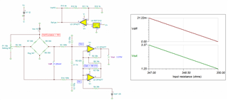
But we observed a loading effect at output pins of sensor and thus a reduction to 3mV from 17mV between Out+ & Out- pins when connected to INA125U IC. 17mV observed across Out +- pins when unconnected to J11(connector to which sensor is connected).

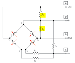
Pressure sensor Wheatstone bridge connections (sensor internal circuitry) is shown below.

What could be the possible issue in this circuitry, do i need to check any impedance control in the path connecting J11 (connector to which sensor is connected) to INA125U input.

Please advice how to fix the same.

  • Hi Bivin,

    have you kept in mind that the voltage reference of INA125 can only deliver about 5mA?

    What is the ref voltage at pin 5 of INA125?

    Why do you have such an extremely high filtering capacitance at the inputs of INA125?? These caps come with such high manufacturing tolerances and drifts that you will totally ruin the balance and symmetry of instrumenation amplifier of INA125. This will result in a heavy degradation of AC common mode rejection. I would remove all these caps and replace them by some well dimensioned and low toleranced NP0 caps.

    Kai

  • Hi Bivin,

    Adding to Kai's comments: Pin5 or IAref pin is required to be low impedance + source/sink Vref voltage, see the attached image below. You may need to use an op amp to drive the node (or reference voltage source/sink IC). You may use a voltage divider and feed into a buffer to configure the Vref. Voltage divider and LDO (only sourcing type) will not meet the requirements. 

    Enclosed is pseudo INA125 Tina simulation. Please see the captured image. 

    INA125 Strain Gauge 03032022.TSC

    In case you'd like to know how to configure differential and common mode LPFs, please see the link below and INA826's EVM in section 3.2.1. 

    https://www.ti.com/lit/ug/sbou115c/sbou115c.pdf?ts=1646336608533&ref_url=https%253A%252F%252Fwww.ti.com%252Ftool%252FINA826EVM

    As Kai suggested, the excitation Vex = 10Vdc reference has to be a separate voltage reference, where 10V/350Ω = 28.6mA (as an example) is unable to be driven by INA125's reference voltage. Unless the load cell's resistance is >> 2kΩ or higher. You could use 10Vdc reference voltage and configure a high output current op amp buffer to drive the wheatstone bridge.  

    If you have additional questions, please let us know. 

    Best,

    Raymond

  • Hi

    1. Regarding the Pin5 or IAref pin connection, we followed the single supply operation guidelines provided in datasheet. In the circuit shared, we provided an optional connection to connect to 10V ref. But if we are not connecting this pin to ground, will it be fine. Please comment.

    2. Also, the R184, R185 outputs of INA125 is connected to ADS7142 ADC in this configuration. Will this create any issue in loading. ADS7142 is operated from 3.3V supply.

    3. You mentioned "reference has to be a separate voltage reference, where 10V/350Ω = 28.6mA (as an example) is unable to be driven by INA125's reference voltage. Unless the load cell's resistance is >> 2kΩ or higher.". Is this applicable to above case of single supply operation.

    Note : Currently this circuit is implemented on card, can i fix loading issue without adding extra opamps or voltage ref drivers.

    Regards

    Bivin

  • Hi Bivin,

    1. Regarding the Pin5 or IAref pin connection, we followed the single supply operation guidelines provided in datasheet...  But if we are not connecting this pin to ground, will it be fine. Please comment.

    I am simulating INA125 with a single supply voltage rail. INA125's Pin5 or IAref node has to be connected to either Ground or a reference voltage. The voltage output transfer function is Vout = (Vin+ - Vin-)*Gain + Vref, where (Vin+ - Vin-) is the differential input voltage of the Wheatstone Bridge sensor, Vref is the voltage at Pin5.

    Vref = 0V if it is connected to GND. As simulated, Vref = 1.25Vdc, and the voltage node has to be a low impedance and able to source/sink in current. 

    Please provide me the maximum differential input voltage from (Vin+ - Vin-)  and the INA125's output range for the strain gauge application (I assumed that it may be for scale measurement application). Assume it is weight measurement application, no weight or load, Vin+ - Vin- = 0mV; At max. weight or load, Vin+ - Vin- = 21.25mV (as an example). Gain per the simulation is configured for 100V/V. Under the max. load condition, Vout = 100*21.25mV + 1.25V = 3.375Vdc, which is shown from the simulation. 

    In the simulation, I placed the strain gauge Rsg on the lower left side. If it is placed upper left side in the location at R7, then you will get (Vin+ - Vin-) = -21.25mV from the configuration. If you reverse the input wire, then the differential input voltage is positive. I am pointing it out in case you get confused. 

    2. Also, the R184, R185 outputs of INA125 is connected to ADS7142 ADC in this configuration. Will this create any issue in loading. ADS7142 is operated from 3.3V supply.

    ADS7142 is SAR ADC, and typically it will require Anti-saliasing filter and kickback LPF filter for sample and hold circuitry within SAR ADC. In terms of loading, it should not be significant, since the input ADC should be a high impedance node. I do not know the ADC product very well and I suggest to contact our ADC support team for assistant.  

    3. You mentioned "reference has to be a separate voltage reference, where 10V/350Ω = 28.6mA (as an example) is unable to be driven by INA125's reference voltage. Unless the load cell's resistance is >> 2kΩ or higher.". Is this applicable to above case of single supply operation.

    Note : Currently this circuit is implemented on card, can i fix loading issue without adding extra opamps or voltage ref drivers.

    The voltage source to source the Wheatstone bridge sensor or load is called excitation reference voltage. It is a high quality, low noise, temperature stable LDO or alternatively, you may use a high current op amp to source the excitation voltage. The output voltage stability and noise level of the excitation voltage source is important, and it may affect your output measurement. 

    Please let me know the resistance of Wheatstone Bridge sensor and I can tell you what you may need. 

    Is this applicable to above case of single supply operation. I am not sure what you mean by applicable. The excitation voltage source needs to be stable, low noise and ripple voltage. I do not recommend switching power supply as a reference voltage. A precision linear voltage regulator or precision op amp buffer circuit should work well. 

    Your system should have operating temperature range. So the excitation voltage has to be able to source the required current for the entire temperature range + some reasonable current margin (normally I will double the current requirements for a given excitation voltage).  

    Please provide me additional details about your design, and I can simulate the circuit to meet your requirements. 

    Best,

    Raymond

  • Hi

    Please find the datasheet of sensor used in link below.

    https://www.mouser.in/datasheet/2/18/1/AAS_920_260C_NovaSensor_NPI_15_102815_web_pdf_3fop-1315847.pdf

    https://www.amphenol-sensors.com/en/novasensor/pressure-sensors/3153-novasensor-npi-15-series-high-pressure-sensors

    Here sensor requires maximum of 1mA and generates a FSO of 100mV, ie maximum input voltage across INA125 input will be 100mV.

    In addition, i'm not measuring transient response of sensor but may read ADC every 0.25 second.

    You mentioned " Vref = 1.25Vdc, and the voltage node has to be a low impedance and able to source/sink in current.", with respect to circuit i shared earlier, which is the voltage node you are referring and what should be the impedance maintained for the same if i'm doing updated layout or routing for board.

    Regards,

    Bivin

  • Hi Bivin,

    Yes, it is easier if I know what type of application and sensor you are working with. 

    This transducer is designed to be driven in constant current. With 1mA of constant current, it generates 200mV differential signal at +Out and -Out nodes.

    Assumed that we are using 200uA constant current, the FSO will 200mV/1mA = 200 = x/200uA, where x=40mV will be generated at the pressure sensor's output at +Out and -Out nodes (assume it is linear). 

    The datasheet did specify nominal 1.0mA, but I am not certain that 1mA is the minimum current requirement or typical current. My guess is that it is a typical. 

     You may use our REF200 as current source or build your own 1mA current source. You may use INA125's 10Vref to drive this sensor in voltage mode, 10V/8kΩ = 1.25mA in each branch (8kΩ||8kΩ), where the total current is 10V/4kΩ = 2.5mA (the bridge impedance is up to 5kΩ per the datasheet). INA125's Vref is able to source the current requirements. 

    I was trying to figure out what the sensor's current consumption is yesterday. Now it is clear that INA125's 10Vref will applicable to the Wheatstone bridge. 

    With 10Vref voltage, the input common mode voltage is configured at 5Vdc. 

    https://www.ti.com/lit/ds/symlink/ref200.pdf?ts=1646338290489&ref_url=https%253A%252F%252Fwww.google.com%252F

    If you want to drive the sensor in constant current, we can discuss it later. 

    Here sensor requires maximum of 1mA and generates a FSO of 100mV, ie maximum input voltage across INA125 input will be 100mV.

    Assume that you FSO is 100mV and 0-100mV corresponds absolute 0-500si as an example (507psi, 1015psi or 5076psi, it claimed there are 4 ranges).    

    If Vout is 3.3V only, then the maximum gain will be 3.3/100mV = 33 V/V, which you selected Rg = 2.2kΩ. 

    You mentioned " Vref = 1.25Vdc, and the voltage node has to be a low impedance and able to source/sink in current.", with respect to circuit i shared earlier, which is the voltage node you are referring and what should be the impedance maintained for the same if i'm doing updated layout or routing for board.

    I am referring to the Vref voltage at the marked red rectangular box, which currently is configured for 4.445Vdc.

    BTW, your output is not ranged from 0-3.3Vdc for ADC sampling. I think that we will need another op amp stage to left shift the INA125's output voltage to 0-3.3V range. We may be able to accomplish this voltage shift in the anti-aliasing filter stage (this is to maximize your ADC input range). 

    The impedance maintained or matching refers to cable length between the pressure transducer and the inputs of INA125 instrumentation amplifier.  You need to use low tolerance resistance and RG gain resistor, prefer to have 0.1% tolerance or better in the differential LPF filter and Gain resistor. The differential capacitor, C1, should be NP0/C0G type or you may use X2Y capacitor. If the design is taken care all these details, the CMRR rejection should be good and will reject most of common mode noises in the pressure sensing application.

    There are some minor details we may need to finalize the IC selection and design. Also, we have many other instrumentation amplifiers for the application. INA125 is good one, since the package has integrated most of the features that you will need. We have other higher performance amplifier that may perform better than INA125 with additional features such as low offset, low drift, high CMRR, wider temperature range etc., but you will need to add other peripheral components. There are pros and cons for the application. If you are interested to know, we can discuss it as well.  

    If you have other questions, please let me know. 

    Best,

    Raymond

  • Hi

    Sorry , i attached link for wrong sensor. The part i'm using is voltage compensated part.

    https://www.mouser.in/datasheet/2/18/1/AAS_920_258C_NovaSensor_NPI_15VC_102815_web_pdf_3f-1389295.pdf

    https://www.amphenol-sensors.com/en/novasensor/pressure-sensors/3149-novasensor-npi-15vc-series-high-pressure-sensors

    We measured current consumed by this sensor on current board, it takes less than 1 mA from 10V reference. But it has an additional series resistor at inputs.

    Regards

    Bivin

  • Hi Bivin,

    ok, the sensor has a bridge resistance of 5k and can easily be driven by the INA125's 10V reference voltage. And you have made the right connections to generate 10V with the INA125. But please remove R189. R189 would short circuit the 10V reference voltage.

    You have decided to run the INA125 in single supply. You can do that, but keep in mind, that the output of INA125 cannot go all the way down to 0V (negative supply rail):

    There are two remedies:

    If you urgently need an output voltage being able to go all the way down to 0V, you can try to power the INA125's negative supply voltage pin by the help of a small negative supply voltage.

    A better option is to shift the output voltage of INA125 into a region where it can operate linearily by adding an offset voltage (called "pseudoground" in the datasheet) to the "IAREF" pin of INA125 of let's say 0.5V. The INA125 emits an output voltage of 0.5V for a zero differential input signal then. And all other output signals of INA125 are shifted by this pseudoground potential as well.

    Keep in mind that when the bridge is generating a negative differential output voltage (think of negative offset voltages coming from the bridge, e.g.), the output voltage of INA125 will fall below this pseudoground potential. So, if you have to deal with AC input signal voltages or negative offset voltages coming from the bridge, the trick with the small negative supply voltage will no longer do, and you might need to choose a pseudoground potential which is way higher than 0.5V, maybe even sitting at middsupply.

    If you want to add a pseudoground, remove R190 and drive the "IAREF" pin directly by the output of an additional OPAmp buffer, similar to figure 2 of datasheet. If you don't have an additional voltage reference chip, you can generate a suited pseudoground potential by connecting a precise resistive voltage divider from the 10V reference output voltage of INA125 to signal ground. Drive the input of a voltage follower (additional OPAmp) with the pseudoground potential and connect the output of this voltage follower to the "IAREF" pin of INA125. Keep the current through this voltage divider sufficiently small, though. No more than 500µA should flow, to not overload the INA125.

    Kai

  • Here are some TINA-TI simulations:

    bivin_ina125.TSC

    bivin_ina125_1.TSC

    Kai