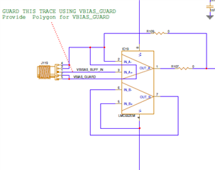
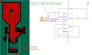
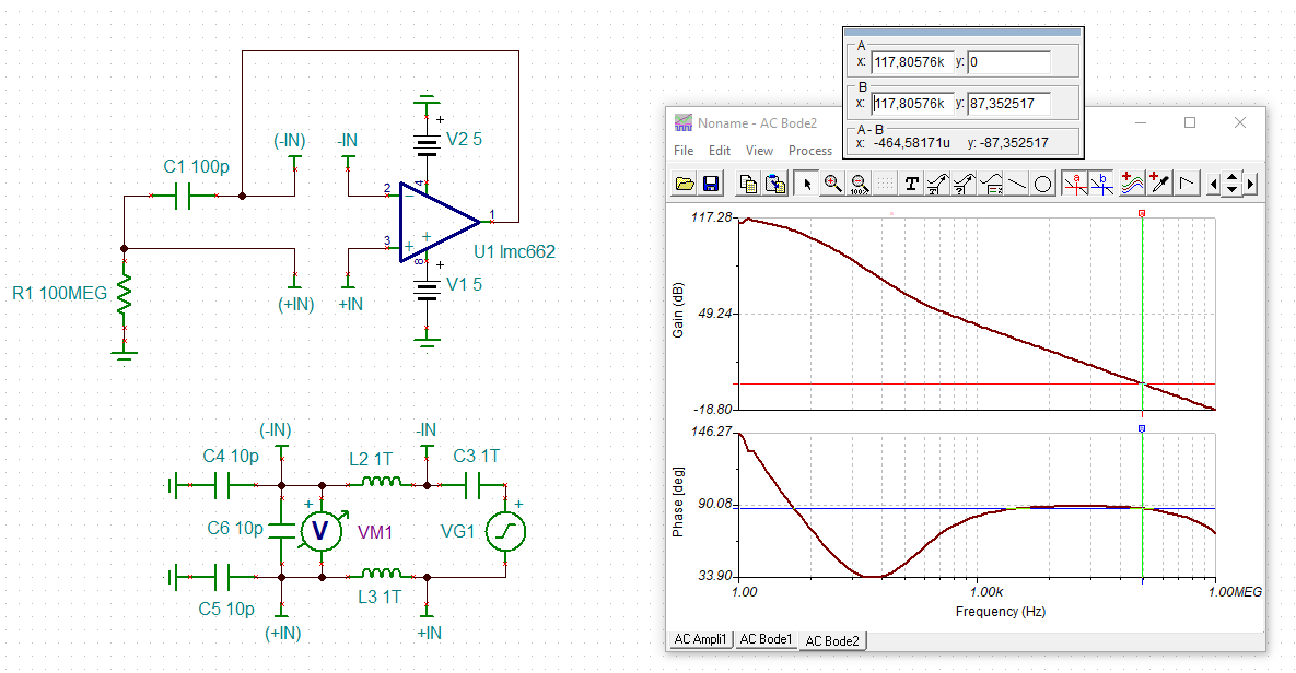
I have an opamp circuit as shown below.
My board stack up is SIGNAL-GND-POWER-SIGNAL.
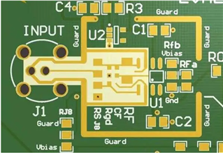
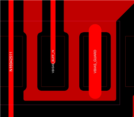
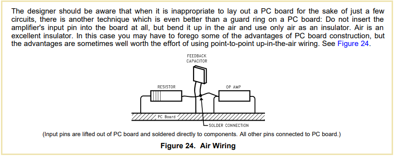
I am providing a polygon to Guard the trace which is going to non-inverting the input of the opamp.
The guard trace is connected to SMA connector also.At present polygon is provided only in the TOP layer(SIGNAL) of PCB
My question is
Do I need to place the Guard polygon in other layers also?
Or can I keep other layers as it is?


