This thread has been locked.

If you have a related question, please click the "Ask a related question" button in the top right corner. The newly created question will be automatically linked to this question.

AMC1200EVM: output/input ratio does not match the specified gain and offset

Part Number: AMC1200EVM
Other Parts Discussed in Thread: AMC1200

I intend to measure the current ( 0.. 2 A ) of a converter driven 3-phase AC Motor

using a shunt  of 0.1 Ohm connected to J2 ( IN1 ) on the board.

For VDD2  5.016 V DC are applied  to J3.

For VDD1 the internal isolation transformer is used ( on JP1  pin2 and pin3 are connected ).

5Viso vs. high-voltage ground is then 5.019 V DC which seems to be correct.

For test purposes I applied different DC current values to the shunt in order to verify

the correct behaviour output vs. input.

I got the following strange results on  J4  (OUT1 ).

( J4 is not connected to any load , pins are blank )

1) IN1 = 0.0 VDC (pins short-circuited ) :

expected voltage on J4 :  +2.50  VDC  ( specified offset )

measured voltage on J4 :  +0.533 VDC

2) IN1 = +0.059 VDC

expected voltage on J4 : 2.50 + 8*0.059  = +2.97 VDC

measured voltage on J4 : -0.147 VDC

3) IN1 = +0.117 VDC

expected voltage on J4 : 2.50 + 8*0.117 = +3.436 VDC

measured voltage on J4 : +0.217 VDC

4) IN1 = +0.235 VDC

expected voltage  on J4 : 2.50 + 8*0.235 = +4.38 VDC

measured voltage on J4 : + 0.915 VDC

Thus the offset is not equal to the specified value of +2.50 VDC.

The gain is not constant and not matching the specified value of 8.

What might be the reason for this strange behaviour ?

Best regards and thanks in advance

Gerhard  Baumann

  • Hi Gerhard,

    It is possible that the input pins are drifting with respect to the high side ground when the external shunt and DC current source are connected. Can you try tying IN- (J2.2) to the high side ground (J1.1) and repeating some of the tests you've conducted? 

    Once IN- is tied to the high side GND. Can you please verify the single-ended input voltage for IN+ and with respect to high side ground at the input of the AMC1200?  

  • Hi , Alexander ,

    thank you for your suggestions !

    I have now resumed my tests :

    On the input side I tied IN1- ( J2.2) to GND1 ( J1.1).

    On the output side I measured OUT1+  (J4.1)  resp. OUT1- ( J4.2)  vs. GND2 ( J3.2 ).

    I got the following results :

    1) IN1 = 0.0 VDC

    J4.1 : + 2.564 VDC

    J4.2 : + 2.504 VDC

    2) IN1 = 0.060 VDC

    J4.1 :  + 2.748. VDC

    J4.2 :  + 2.324 VDC

    3) IN1 = 0.116 VDC

    J4.1 :  + 2.916. VDC

    J4.2 :  + 2.155 VDC

    4) IN1 = 0.233 VDC

    J4.1 : + 3.252 VDC

    J4.2 : + 1.820 VDC

    My conclusions are :

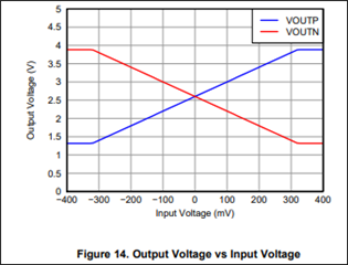
    OUT1+ and OUT1- have a gain of 3 vs. IN1 , which is approximately

    corresponding to the curve in figure 14. but is not matching a gain of 8 mentioned

    in the manual.

    For IN1 = 0 V ( measuring 1 ) both outputs are expected to have the identical

    offset of 2.5 V but there is a difference of  60 mV which seems to be too high.

    I am looking forward to your comments.

    Best regards

    Gerhard Baumann

  • Hi Gerhard,

    The gain of 8 corresponds to measuring the output differentially. i.e. (J4.1-J4.2)/IN1 = Gain. However, the value is changing significantly over the sweep and the initial offset is incorrect like you said. 

    Can you tell me a little bit more about your signal source? Is it set to a high impedance output and are you using an additional DMM to verify the voltage on the input pins?

  • /cfs-file/__key/communityserver-discussions-components-files/14/Messung.pdf

    Hi , Alexander ,

    thank you for your comments.

    Via the link above you will see my test arrangement.

    The signal source output impedance is the 0.1 Ohm resistor which should be low enough.

    For the voltage measurements a DMM Fluke 175 is used ( input and output ) which has an

    input impedance of  > 10 MOhm.

    Using an oscilloscope for additional measurements I found that there is a minor high frequency

    noise signal ( approx. 12 mV r.m.s. / 10 MHz ) on the output of the 5 VDC power supply.

    I can see this noise on J2.1/2 as well as on J4.1/2 but I don't think that this will cause my problems.

    Best regards

    Gerhard Baumann

  • Hi Gerhard,

    Thank you for the drawing and additional information. Your test setup looks very robust and my only concern is that the power supply ripple is seen on the inputs J2.1/2 and then the output. The anti-aliasing filter cutoff frequency is high by default, approximately 20MHz. Replacing C3/8 with a 10nF capacitor to reduce the cutoff frequency to 600kHz may help attenuate this noise. However I agree this should not cause problems with both inputs (J2.1/2) tied together and to GND1 (J1.1); you should only see the specified common-mode output voltage of 2.5V on both outputs with a differential voltage less than the specified offset voltage. If this is not the case, it is possible that the device has been damaged, perhaps due to ESD. 

    Just to confirm, are you using the RevB board with the additional AMC1200 in the DWV package as well?

    Is it possible to test tying the inputs together and to GND1 with that package? 

  • Hi, Alexander,

    thank you for your hints .

    My board is of type AMC1200BEVM Rev. B.

    It has two channels with two different amplifier package types  :

    U1 is of package type DUB ,

    U2 is of package type DWV.

    So far I had used U1 only , but I changed now to

    the channel with U2 (J5 vs. J6) and I got the

    following results :

    1) IN2 = 0.0 VDC (pins short-circuited)

    J6.1 vs. GND2 : +2.522 V

    J6.2 vs. GND2: +2.523 V

    2) IN2 = 0.060 VDC

    J6.1 vs.GND2 : +2.760 V

    J6.2 vs. GND2 : 2.284 V

    3) IN2 = 0.119 VDC

    J6.1 vs. GND2 : 2.997 V

    J6.2 vs. GND2 : 2.046 V

    4) IN2 = 0.235 VDC

    J6.1 vs. GND2 : 3.462 V

    J6.2 vs. GND2 : 1.580 V

    My conclusions are as follows :

    a) the gain for the differential signal (J6 vs. J5) is exactly 8 as it should be.

    b) the gain for the single ended signals ( J6.1 resp. J6.2 vs. GND2 ) is exactly +/- 4 as it should be.

    c) The offset voltages on J6.1 and J6.2 for IN2 = 0V are identical. So it

    doesn't  matter that they are not  exactly 2.50 V.

    d) It did not make any difference if J5.2 was tied to GND1 or not.

    The voltage on J6 remained unchanged , as it should be.

    Obviously the amplifier U1 seems to be damaged , possibly due to ESD as you assumed.

    Maybe I was not careful enough during the wiring.

    Amplifier U2 works completely correct. So I can comtinue the tests because

    I need one channel only.

    Thanks again for your support

    and best regards

    Gerhard Baumann

  • Hi Gerhard,

    I'm happy to hear that the second channel is working correctly and thank you for the debug. 

    Please let me know if you have additional questions. 

  • Hi , Alexander,

    I shall now continue with my tests. At the moment I don't see

    further problems. So  I think we can close the thread.

    Best regards

    Gerhard Baumann