This thread has been locked.

If you have a related question, please click the "Ask a related question" button in the top right corner. The newly created question will be automatically linked to this question.

AMC3330: using AMC3330 at current sensing loop

Part Number: AMC3330
Other Parts Discussed in Thread: ISO124, AMC3301,

Dear experts,

We have an application and are finding the other solution for that.

The original design is 2 kinds of current sensing switched by rely: one using 100ohm sensing 15mA and the other 100kohm sensing 15uA using LTC6090+ISO124.

The problem is ISO124's bandwidth is not enough so their feedback loop could not react timely.

We found the solution AMC3301 could only support +/-0.25Vin and it's not enough to support their current input range(100ohm x 15mA=1.5V) and AMC3330 could support +/-1Vin which is more close to current design.

Thus, we have 3 questions need to be answered to help us know if we could use AMC3330:

1. Could AMC3330 be used as current sensing by using 66ohm or 66kohm to sense 15mA and 15uA respectively?

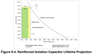
2. Could AMC3330 input sustain 1200V DC because their input common mode will be operated at 1200V?

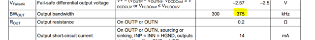
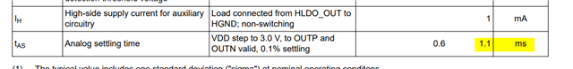
3. We hope to find a solution with bandwidth > 300kHz and we found AMC3330 could support this. However, we found that the analog settling time tAS is 1.1ms max. This will affect the output settling speed and 1.1ms is too slow for us so we still could not use it at our feedback loop, right?

Thank you.

Best Regards,

Cindy

  • Hi Cindy,

    1. Yes, this would be OK. The resistor can also be sized to the 250mV input range of the AMC3301. 

    2. The high side ground must float with the inputs as well such that the input common-mode voltage specification is not violated. This is often accomplished by connecting HGND to INN as shown in the datasheet. The working voltage is specified to 1700VDC as shown in the picture you posted. Figure 6-4 shows the lifetime projection vs applied voltage. 

    3. This specification is how long the device takes to power up when the VDD voltage on the low side is applied, not for a step response on the input pins. The specified behavior for a step response on the input pins is shown in section 6.10 and 6.11 below. An application curve for the same is shown in section 8.2.3. Does this answer their question or is it in regards to the turn on time for the device? 

    Please let me know if this helps or if you have additional questions.