This thread has been locked.

If you have a related question, please click the "Ask a related question" button in the top right corner. The newly created question will be automatically linked to this question.

OPA855-Q1: Output layout instruction

Part Number: OPA855-Q1
Other Parts Discussed in Thread: OPA855, LMH5401

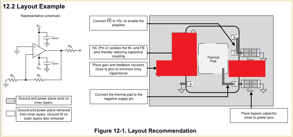
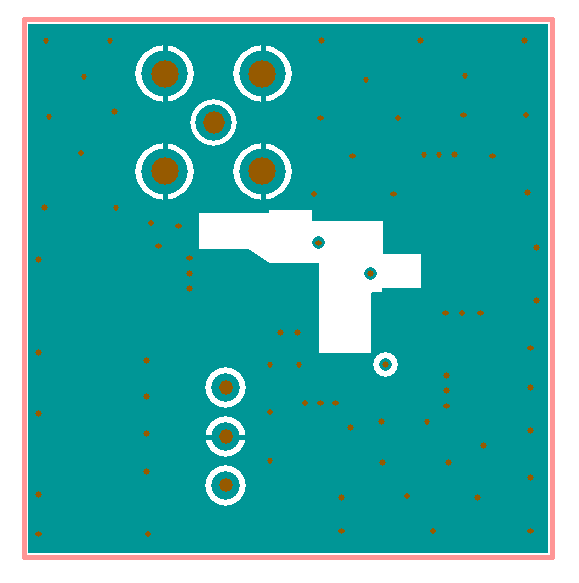
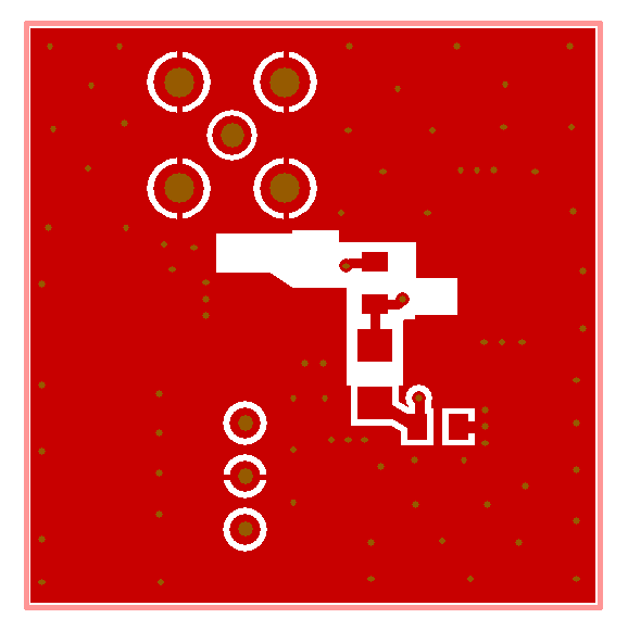
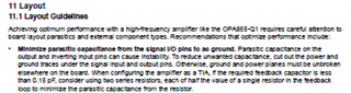
The layout guidance provided in the OPA855 data sheet is to remove ground planes under all input an output pins.

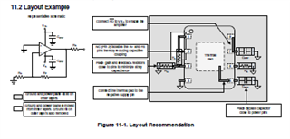
The Figure below the text only shows a cutout in the region of the FB pin only.

Should the actual output pin also have the cutout to reduce parasitic capacitance?

  • Hello Francis,

    You have asked a good question!  Layout is a critical part of high speed design and you are right to explore what amount of GND & power plane cutouts are recommended for your application.  While I acknowledge the difference between Section 11: Layout Guidelines and the accompanying image, I would argue the text description should be prioritized over the image in your analysis.  I looked over the EVM board for the OPA855 and the layout for the EVM shows the GND and power plane cutouts on pages 4 & 5 of the EVM User Guide. 

    https://www.ti.com/lit/ug/sbou210/sbou210.pdf

    Combining the advice between the written 11.1 Layout Guidelines section, the 11.2 Layout example and the OPA855 EVM, you are advised to also cutout the output & input, not just under the feedback resistor/pin. 

    In short, I recommend the input & output pin/network cutouts to reduce parasitic capacitance, as you mentioned in your question.

    Best,

    Alec

  • Hi Francis,

    this is how I usually make openings in the ground plane of a HF circuit:

    The openings should include the area under the solder pads of all involved components (OPAmp, feedback resistors), the area under the involved copper tracks and the area under the involved components. See the red rectangles. You will notice that the openings are a bit wider than what is actually consumed by the solder pad, copper tracks and components.

    The openings should be made at least in all the upper layers of printed circuit, namely the ground fill layer on top of the printed circuit board and in the inner layers. Whether the openings should also be made in the bottom layer of printed circuit board depends a bit on the application and the used OPAmps. In my 27MHz sensor circuits where three 1GHz OPAmps are used, I don't make openings in the ground plane of bottom layer, because I need this solid ground plane in the bottom layer as a shield against other circuitry. But this cannot be made with all OPAmps. Some even need the openings also in the bottom layer.

    It's interesting to note, that the layers of a multilayer board are not equally spaced, usually. In many 1.6mm thick 4-layer-boards, for instance, the distance between the inner layers and the outer layers is only about 100µm. So, the stray capacitance formed between the top layer to the second layer is 1.6mm / 100µm = 16 times bigger compared to the stray capacitance between the top layer and the bottom layer!!! This is a huge difference and because of this it's a must to have openings in the second layer of a 4-layer-board. In a multilayer board the distance between the top layer and the second layer can even be less than 100µm.

    This huge difference is the reason why openings is a "must have" in the inner layers, while a solid ground plane in the bottom layer without openings can be accepted in certain applications.

    For the same reason, don't forget openings in the solid ground plane under ferrite beads! A 100µm spaced ground plane would otherwise very effectively short-circuit the ferrite bead and totally ruin the filtering performance. The same is true for copper tracks which are running 100µm under the OPAmp in the second layer. The stray capacitance here can totally ruin the performance of OPAmp and even cause instability. Always have an isolating ground plane between copper tracks running in different layers. Or, saying the same by different words, never allow a signal to cross an opening in the ground plane.

    Because of the huge stray capacitance between the top layer (component layer) and the second layer of a multilayer board, even other components (and copper tracks !) which seem to be less vulnerable should have an opening in the solid ground plane. But I think it's no good idea to make the opening wider than absolutely neccessary. And I think it's a good idea to think about having a solid ground plane in the bottom layer, which is 16 times farer away from the top layer than the second layer. My circuits have definitely profited from it.

    What is also not shown in figure 12-1 is the many vias which are neccessary to connect the individual ground planes and ground fills with each other. The following example layout which I made earlier for another thread, shows a minimum number of vias:


    Another important tipp: Never place the components of a HF circuit just where free place is available. Always place the components at their ideal positions (shortest distances of the signal routing at the -input of OPAmp, shortest ground connections, shortest connections between the decoupoling caps and the supply voltage pins, etc.) and then move the whole block to a free position on the printed circuit board. You will miserably fail when you start to pull apart the components in order to fill unused areas of the printed circuit board or to make the layout look more lovely. You can do this with a 1MHz OPAmp, to some degree, but definitely not with a 1GHz OPAmp. Even every millimeter copper track counts. A 1cm long and 0.3mm wide copper track shows an inductance of about 10nH and a stray capacitance of about 1.2pF. 10nH equals an impedance of 63R at 1GHz and 1.2pF equals 133R at the same frequency. So this short copper track behaves as if you would install an additional 63R and 133R impedance into your circuit. Do you think this would be a good idea? But you effectively do it when rooting such a 1cm long and 0.3mm wide copper track in your circuit.

    A copper track running over a ground plane develops a characteristic impedance. If the copper track is becoming longer and longer, microstrip techniques should be used to make the copper track look like a 50R line in a 50R system, e.g., in order to be able to terminate the line properly with its characteristic impedance. But that's a different story.

    Kai

  • Thanks Kai for the information,

    I cutout all layers around the FB pin and and feedback components in my OPA855 TIA design similar to your recommendation.  Also followed other recommendations of keeping the APD and feedback network very close to the OPA855. Phase margin using PSPICE and Tina Spice >> 45 degrees.  There have been no stability issues and we have built thousands of boards to date with no stability issues. 

    The reason for the post is that I am working on a new version of the detector for another system and I saw a discrepancy between the layout recommendation text and the figure in section 11 of the OPA855 data sheet.

    There are some high(GHz regime) bandwidth amplifiers where clearing out the ground at the input and output pins results in excessive inductance and is not recommended. (i.e.) LMH5401

    For this design my singled ended impedance is 50 ohms. My differential impedance traces are 100 ohm.

    Question:  Do you know why adding the ground under the FB pin would affect stability?  I can see where it would affect bandwidth and input referred noise but I am not sure how it affects stability.

    thanks,

    Frank

  • Hi Francis,

    the main advantage of having a separate FB pin on the same side as the -input pin is to minimize the copper track parasitics (inductance and stray capacitance) of the feedback resistor connection to the output of OPAmp. And as the FB pin is internally connected to the output of OPAmp, a subjacent ground plane would increase the load capacitance seen by the output of OPAmp. This does have a negative impact on the phase margin, not much in the simulation, but not negligible either: 

    Stray capacitance at the -input of OPA855 does have a way more negative impact on the phase margin, though:

    francis_opa855.TSC

    I think that the opening in the ground plane in figure 11-1 of datasheet has accidently slipped upwards a bit. At least, the corresponding text in the datasheet is in contradiction to figure 11-1, as it clearly says that ground should be removed under the input and output pins. I think the intention was to place the opening in the ground plane directly under the feedback resistance RF, also covering the copper track going to the -input of OPAmp (pin 3). But even then, the opening would be incomplete as it doesn't cover the "hot" solder pad of Rg and the solder pad of the -input of OPAmp (pin 3).

    I think my openings are better Relaxed

    There are some high(GHz regime) bandwidth amplifiers where clearing out the ground at the input and output pins results in excessive inductance and is not recommended. (i.e.) LMH5401

    A small resistor in the range of 10...100R in series to the input of OPAmp and installed directly at the input pin can often help. The idea of this resistor is to dampen resonances caused by parasitics (bond wire inductance, stray capacitance, etc.). The resistor can also act as a light low pass filter in combination with the input capacitance of OPAmp. Heavy enough to prevent the input stage of OPAmp from oscillating but light enough to avoid relevant bandwidth limiting of the whole circuit.  

    Kai

  • Thanks Kai -

    Makes sense.

    Essentially you are adding capacitance to the output and therefore reducing phase margin

  • Exactly, Francis Relaxed

    Kai