Because of the Thanksgiving holiday in the U.S., TI E2E™ design support forum responses may be delayed from November 25 through December 2. Thank you for your patience.

This thread has been locked.

If you have a related question, please click the "Ask a related question" button in the top right corner. The newly created question will be automatically linked to this question.

LOG101: Schematic and PCB layout guard rings

Part Number: LOG101

Hello E2E,

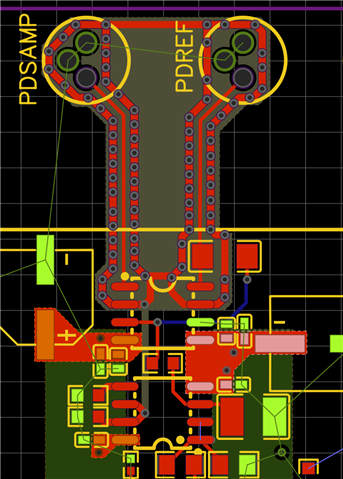
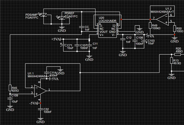
Our customer would like to request verification before they run the schematic and PCB layout for the guard rings.
The LOG101 connects to two photodiodes, guard traces are shown wrapping around those terminals through the NC pins.  The guard trace is driven from a unity gain op-amp (SO8 below the LOG101) whose non-inverting terminal is connected to the ground through a 100ohm resistor.  If you need other details, please let me know.
Regards,
Carlo

  • Hi Carlo,

    why no simply connecting the guard to signal ground (pin 6 of LOG101)?

    You could even use individual guards for each input.

    Kai

  • Hi Carlo,

    Guard rings are critical on logarithmic amplifiers or transimpedance applications where the user need to measure very small currents in the lower pico-ampere range.  The LOG101 specifies a dynamic current range from 100pA to 3.5mA. Although this current range is still relatively low, the guard ring may not be as critical.

    Nevertheless, the guard ring will still provide shielding to GND on the signal path input traces, helping reduce noise pick up and improve EMI rejection.   

    As Kai has mentioned, you may consider connecting the guard ring directly to GND, since the internal LOG101 non-inverting inputs are referred to the same GND potential, and you may not require buffer U1.2 driving the guard rings.

    Another factor to consider is to ensure the PCB board is completely clean and free of flux residue and contaminants prior performing low current measurements.  On our evaluation, the boards are cleaned from flux using an ultrasonic deionized water bath clean for 15 minutes to ensure complete removal of the flux underneath the devices. However, in your PCB, the appropriate flux removal process may vary depending on the type of flux used.

    Thank you and Regards,

    Luis