This thread has been locked.

If you have a related question, please click the "Ask a related question" button in the top right corner. The newly created question will be automatically linked to this question.

OPA277 lead compensator resonant artifacts

Other Parts Discussed in Thread: OPA277, OPA132, OPA140, OPA656, OPA727

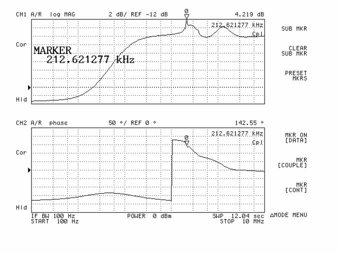
1.       Attached is a simulation of a simple lead compensator built around the TI OPA277. It is exhibiting spectral peaking ~500kHz in the pass band. Actual measurements reveal this artifact occurs ~212 kHz. I have been unable to explain this phenomenon (originally I thought it was parasitic capacitance de-stabilizing the response) but the fact that the resonant behavior  is present on the simulation leads me to believe it is related to the open loop response of the 277. Equally important, what means can be used to correct the resonant peak?

2.       Are you familiar with the term “semi-differential” as relates to signal propagation? How is it different from true differential propagation? How is it typically implemented? How does it’s common  mode rejection differ from true differential mode?

Thanks
  • Eric,

    The feedback network of an op amp is a load on the output of the amplifier. Imagine that the input voltage source is zero impedance (a short) and the feedback network looks like two series resistors and two series capacitors. The capacitors are a 5nF load on the amplifier. This is too much capacitive load for this op amp.

    Check the typical curve in the upper left hand of page 8 of the data sheet. You see that the overshoot is off the chart for a 5nF load. This would mean you will get severe peaking or oscillations.

    You can probably achieve the same desired transfer function by scaling the impedance of the network up by 10x or so. This would be an equivalent 500pF load.

    Sorry, but I am not familiar with the term "semi-differential." If you can provide more details, maybe we could help.

    Regards, Bruce.

  • Thank you for the response Bruce. I tried scaling and now I am observing a giant suck out after 212kHz. Any idea what the source of this is and how we could possibly correct?

  • Eric,

    I didn't know what type of fidelity to the close loop network response you really need. I believe that you are probably just running out of bandwidth on the amplifier. The OPA277 is a 1MHz device. At high frequency, you are in a noise gain of 2 so you have precious little loop bandwidth to assure fidelity to the closed loop network response. With the 500pF load capacitance and little loop gain, the 100kHz+ region is going to be marginal. You probably need to move to an op amp with higher gain-bandwidth.

    I'm not sure about your simulator. You probably have a idealized op amp model. You can adjust the gain-bandwidth to see its effect on your closed loop response. A general model will not, however, do so well at modeling the effect of open-loop output Z interacting with the 500pF load. You could try the OPA132 or OPA140 macromodel and see what you get.

    Regards, Bruce.

  • Thanks Bruce,

    Switching to the OPA656 solves the problem

  • Sorry, one last question- I am designing an integrator using the OPA277. The cross over frequency is 1 Rad/sec. I am using a 10uF cap and a 100KOhm resistor.  The Tina model predicts a significantly underperforming gain near DC (e.g. I thought I would expect to see ~150dB the open loop gain). I have yet to validate in the lab. I did however replace the opa277 with an opa656 in the simulator and it seems well behaved (i.e. near DC it is at ~60 dB, the open loop gain of the part). Again I haven’t validated in the lab yet , but what would account for this?

  • Eric,

    The typical gain of the OPA277 is listed as 140dB. Minimum is 115dB for the low cost gradeouts. There probably is not much attention paid to accuracy of the model in this respect. Once the gain is in the 120dB region, other errors such as noise, offset, drift tend to dominate. What gain do you see? In your application, there is probably a greater potential error due to input bias current due to the 100k resistor.

    Regarding the op amp selection for the lead circuit, you might want to check the OPA727. It operates on +/-5V and has 20MHz GBW. The OPA656 seems like overkill for GBW.

    Regards, Bruce.


  • Thanks Bruce,

    Responses in Red

    The typical gain of the OPA277 is listed as 140dB. Minimum is 115dB for the low cost gradeouts. There probably is not much attention paid to accuracy of the model in this respect. Once the gain is in the 120dB region, other errors such as noise, offset, drift tend to dominate. Agree What gain do you see? But the TINA simulator craps out at -4dB at  ~50mHz?? (see attachment) In your application, there is probably a greater potential error due to input bias current due to the 100k resistor. Perhaps. Lab results look for encouraging. The thrust of my question is why the simulator can’t get above -4 dB but has no problem when an OPA 656 is dropped in (which yields close to its predicted 60dB open loop gain. Why doesn’t the simulator work on the 277. Not even close)

    Regarding the op amp selection for the lead circuit, you might want to check the OPA727. True, but I don’t have any engineering samples. I have plenty of 656’s to play with It operates on +/-5V and has 20MHz GBW. The OPA656 seems like overkill for GBW. 

    I can get samples for them to play with.

  • Eric,

    I believe that you have done an AC analysis with the output of the op amp locked in the positive rail. Do a DC analysis... calculate nodal voltages. I think you will see that the output is in the rail. The input bias current of the op amp is driving the output into the rail.

    The FET input op amp model probably has zero or near zero input bias current. The model's diff input resistance keeps it biased in the linear range.

    Beware of SPICE artifacts and check DC operating points.

    Regards, Bruce.

  • Thanks Bruce,

    I received some more info on the semi-differential question..

    I am also unfamiliar with the term sem-differential.  I first learned of the term as a proposed approach to reducing common mode noise by a Honeywell partner company (please see attached schematic).  Can you please comment on this design? I am still skeptical and must confess I don’t understand how true differential mode is supported (it seems that all that is being done is passing a common ground between both circuits). Additionally it would seem to me that this design is at risk of introducing more noise because of the added op amp at the receiver! Any feedback that you and your team could offer would be greatly appreciated.


    Thanks,

     6303.TIA_LCM_Differential_Scheme.pdf


  • Eric,

    This "semi-differential" approach has some merit. It senses the signal differentially, referring the signal to the specific ground point for one given amplifier. If you have a large board with many signals, ground on that board will not be the same voltage everywhere. This scheme allows you to measure with respect to the ground point of one particular amplifier.

    Regards, Bruce.

    BTW... did you solve the issue with the OPA277 integrator? I simulated it using a commonly used trick to bias the integrator in the linear range and got the proper open-loop gain.

  • Sometimes this is simply called "remote ground sensing". It is a perfectly valid technique, Eric.

    Regards, Neil P. Albaugh   ex-Burr-Brown

  • Yes,

    Your advice solved the problem.  Thanks for all the support.