This thread has been locked.

If you have a related question, please click the "Ask a related question" button in the top right corner. The newly created question will be automatically linked to this question.

LMH6503: LMH6503

Part Number: LMH6503
Other Parts Discussed in Thread: VCA822, VCA820, VCA824

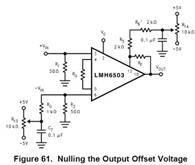
Hello, on page 19 of LMH6503 daatasheet, Figure 61 shows how to adjust (on pin 12) the output offset of the LMH6503 IC. Can this adjustment be useful to adjust the offset from 0Vdc to +/- 5 Vdc when the LMH6503 is powered at +/- 12V? Thanks.

Regards

  • Hi Fulvio,

    this scheme is intended to null the offset voltages. As voltage controlled gain stages usually react very sensitively to offset errors, I don't think that the nulling scheme can be used to create such a high imbalance. This would be just the opposite of what one would want to achieve with the nulling scheme.

    Kai

  • Hello Fulvio,

      Page 19, Figure 61 of the LMH6503 datasheet demonstrates how to nullify the offset voltage by adjusting resistance via trim pot to adjust the voltage applied to the input of the amplifier in order to "cancel" the amount and the lower the amount of output offset voltage of the device. Figure 37 to Figure 43 are important figures that go along with this section. 

      As Kai pointed out, this is the opposite of what you would want for your design. You can apply a DC bias at the non-inverting input of the amplifier similar to biasing a standard amplifier as shown below or via voltage divider (be careful with bias current of the amplifier).

       Also, LMH6503 can not be powered with a +/-12V power supply. The maximum Vs of the device is 12V. Did you mean to set configuration to 12V single supply with 5V DC common-mode voltage? 

    Thank you,
    Sima 

  • So Fulvio, 

    The LMH6503 is the VIP10 (National Semi, Arlingtone fab originally) lineal descendent of the Lucent CBICU (Reading, PA) CLC522. We did that and the CLC520 (dB/V adjust) long ago at Comlinear (Steve Smith IC designer) where those have been migrated in the BurrBrown CBC10 process (Tucson) through to the VCA820 and VCA822 where this latter is the LMH6503 equivalent. They all share a similar internal block diagram with an input differential transconductance stage where that signal current is modified through the gain control to an on chip CFA based transimpdedance output - that CFA output was used for slew rate but I always wanted to do a decomp VFA for that to get better noise - never happened. 

    Anyway, Figure 61 is just showing a summing current input path into the inverting input of the output CFA amp - not showing (but has to be there) the V+ node on that amp at ground usually. Since this adjustment is just another signal path into the inverting summing junction of the output op amp you can use it to adjust the output DC anywhere inside the output range. And yes, these are on 14V kind of breakdown processes, so typically +/-5V or +/-6V supplies. We did faster versions of the VCA as well in CBC10, I think the VCA824 is one of those. 

  • Good to have you here, Michael Relaxed

  • Thanks Kai, sometimes these questions overlap the parts I worked on, so easy to fill in the details. The original CLC520 and CLC522 consumed a lot of my time in their release - made a pretty detailed effort at a new noise model for this type of part, that sits inside the old CLC522 or CLC520 datasheet, but I don't think anyone brought that forward in the later parts - the gain control gave an interesting peak in noise (flatband) around 6dB attenuation I vaguely recall. Countless hours of taking data and postulating an equivalent model there. 

    And of course when we bumped up against parasitic oscillations, those things you don't forget - the original parts had a 1.2GHz self oscillation in the input stage of the output op amp if you just grounded that V+ input - hence, the datasheets I did showed a 20ohm external to ground there to deque that emmitter follower oscillation. 

  • Hello, thanks Sima for the reply.
    Ok about the offset, but in the datasheet on page 3 it is specified: "Absolute Maximum Ratings Supply Voltages (V + - V−) = 12.6V", therefore the dual power supply applicable to the LMH6503 can also be (V + - V−) = 12 V, which is less than the Absolute Maximum Ratings Supply Voltages (V + - V−) = 12.6V. In fact, in the case of power supply not exceeding V + - V− = 5V, the value should be: "Absolute Maximum Ratings Supply Voltages (V + - V−) = 5.6V or 6V".

    Thank you,

  • Hello Fulvio,

      That is correct, (V+ - V-) must be less than 12.6V to avoid damaging the device. The original question listed power supplies at +/-12V (Vs+ = 12V and Vs- at -12V) which would equal to a differential supply voltage of 24V. 

    Thank you,
    Sima 

  • Ok, sorry, I had interpreted (V + - V-) as (V + / V-) dual power. Is there a chip equivalent to the LMH6503 (LMH6503MA / NOPB package since I already made the PCB) that can be powered at + 12V / -12V or + 15V / -15V?

    Thank You

  • there is not, you should change your supplies - if you need more swing, you will need another postamplifier on +/-15V supplies, here is a short selection table of single CFA higher voltage options, 

  • Hello Fulvio,

      Here are additional high supply PGA/VGAs: https://www.ti.com/amplifier-circuit/pga-vga/products.html#p358max=24;36

    Thank you,
    Sima