This thread has been locked.

If you have a related question, please click the "Ask a related question" button in the top right corner. The newly created question will be automatically linked to this question.

LMC6042: How to give the guard ring for smd pack for protect the high impedance sensitive signals from leakage current.

Part Number: LMC6042
Other Parts Discussed in Thread: LMP7721

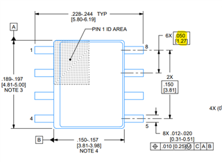
since 15 years we are using one LMC6042  through hole component in existing system, but i do not know how to give the guard ring for smd pack. i would like know how to give the guard ring  for smd pack.

If i go same part of SMD shall i use same guard ring? or need to change anything? please give me some guide .....if i go smd pack instead of throgh hole.

  • Thirumal,

    Please see the below guidance for guard ring on surface mount devices. The summary is that you only need a guard ring on the layer the trace exists, the PCB makes a good enough insulator between the bottom layer.

    https://e2e.ti.com/support/amplifiers-group/amplifiers/f/amplifiers-forum/58275/guard-ring 

    Best,
    Jerry

  • Hey Thirumal, 

    Please also see pages 11 and 12 of the datasheet for the guard ring recommendations/air wiring. The distance in the SMD is plenty for guarding clearance. 

    All the best,
    Carolina

  • Hi 

    Thanks for your valuable reply!

    In data sheet providing every  information only for through hole components not for complete smd pack. 

    We can give air wiring /guard ring top and bottom  for through hole components  but  we can give the guard ring on the top layer  for smd but   we  can not give air wiring for smd. Without air wiring is it create any issue ? and is it enough guarding clearance for using SMD part. 

    Because we are using high sensitive or high impedance signal interfacing (p02,lac,glu)to LMC6042.

  • Hi

    Thanks for your information!

    See am asking guard ring for smd pack.....the given information everything is through hole guard ring.

    Thanks,

    Thirumal K

  • Thirumal,

    The summary is that you only need a guard ring on the layer the trace exists, the PCB makes a good enough insulator between the bottom layer.

    The guidance for SMD guard ring is almost the same as the guidance for through hole guard ring, however you only require the guard ring on the layer the SMD is on, as the PCB will make a sufficient insulator between the top and bottom of the board.

    Best,
    Jerry

  • Hi Thirumal,

    as Carol already mentioned there's enough space for the guard ring between adjacent solder pads. Distance between adjacent solder pads is 1.27mm. Recommended width of solder pads is 0.6mm. Additionally subtracting two times the clearance of solder mask of 0.05mm gives a solder mask bridge of

    1.27mm - 0.6mm - 2 x 0.05mm = 0.57mm

    Even with a clearance of 0.07mm the soder mask bridge will be 0.53mm. This is fully enough for almost all manufacturers of printed circuit boards.

    And you can easily place a 200µm wide copper track under this solder mask bridge between adjacent solder pads. 0.53mm - 200µm = 2 x 165µm resulting in a 165µm solder mask overlap at both sides of this 200µm wide copper track. This is also what an usual pcb manufacturer can easily make.

    Of course, if you are not willed to use a solder mask, serious issues can occur durign the soldering Relaxed Then you would profit from taking the LMC6042 in the DIL8 package or from taking the LMP7721 with the special pinout.

    Kai