This thread has been locked.

If you have a related question, please click the "Ask a related question" button in the top right corner. The newly created question will be automatically linked to this question.

THS4551: Noise analysis from SLOA054E

Part Number: THS4551
Other Parts Discussed in Thread: THS4531A, TINA-TI

Hello,

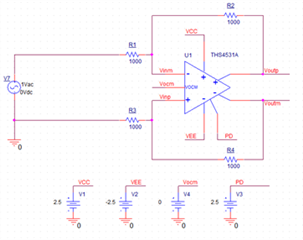
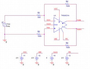
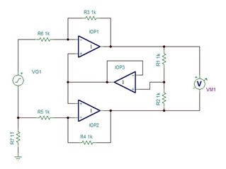
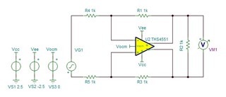
I have one question related to the noise analysis on the THS4551 (but question is related to all FDA I guess).

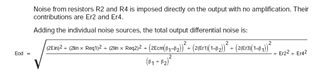
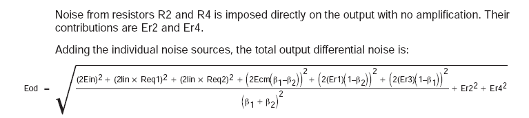
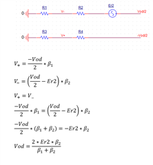
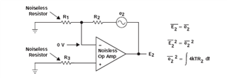
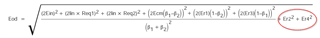
I'm trying to calculate the noise gain when resistors aren't the same. Regarding the SLOA054E by James Karki, result is 2 / (Beta1 + Beta2).

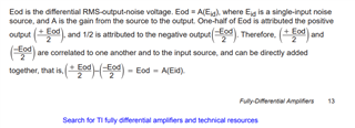
I understand the calculation made on the SLOA054E but I don't understand why one half of Eod is attributed to each single ended on page 13.

1/ Is is just to simplified the calculation?

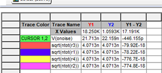
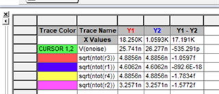
2/ In the real life, if I measure the differental noise, it will be the same than measured on each single ended output but multiplied by around sqrt(2), Am I wrong?

3/ Is it possible to calculate the noise gain using equation of §8 (like equation 15)?

Many thanks

  • Hi Matthieu,

    here's another appnote on noise of fully differential amplifiers:

    snoa506a.pdf

    Kai

  • Hi Kai,

    Thanks for your feedback. Nevertheless, I already read this appnote but I'm searching to understand the noise equation with unbalanced feedback resistors.

    SLOA054E is the unique appnote I have found for this, very useful but confusing for me at the start point when attributing one half of Eod to each single ended.

    Matthieu

  • why would you imbalance them, that will create a number of artifacts like input to CM conversion. 

  • Hi Michael,

    I don't really want imbalanced the feedback network but I would like to understand generic equation given in SLOA054E and their start point.

    Matthieu

  • Of the few folks focused on FDA collateral, only Karki felt inclined to pursue theoretical mismatch issues - interesting, but not overally useful to end apps. 

  • Ok, I understand. Again two questions.

    1/ In the real life, if I measure the differental noise, it will be the same than measured on each single ended output but multiplied by around sqrt(2), right?

    2/ So it is possible to calculate the noise gain using standard equation by regarding Vout_diff / Vin+, right? I know the result is 1 + Rf/Rg but how calculate it, is it like a standard inverting amplifier where V+ = V-?

    PS : Is it possible to contact Karki?

    Matthieu

  • Hello Matthieu,

      1. That is correct. The THS4551's datasheet has a noise analysis section which shows the main terms and shows how individual noise sources contribute to final estimated FDA noise:


        Also, here is standard vs FDA noise analysis circuit:


      2. The noise gain of FDA is the same as for standard amplifier. This video series (videos 1 and 2) shows a step-by-step on how the noise gain is calculated for FDAs:

         training.ti.com/ti-precision-labs-op-amps-fully-differential-amplifiers-introduction-fdas-and-differential

  • Hi Matthieu,

    the noise specification of datasheet is gained by using a circuit with balanced resistors. As the output noise is the complex sum of correlated and uncorrelated noise and changing from balanced resistors to unbalanced resistors would alter the mix of these noise sources, the noise specifications given in datasheet would no longer be valid when changing to unbalanced resistors.

    This is no true limitation because it makes no sense to run a FDA with unbalanced resistors anyway.

    Kai

  • Ok Matthieu, I didn't really want to look at it but here I think is the page 13 section you are having trouble with, 

    Karki is kind of bouncing back and forth between flat spectral noise and RMS noise. However when says what is below, I think he meant to indicate that 1/2 of the output Vpp noise (taking the differential RMS times noise power bandwidth) is on each output - by definition, going from differential to single ended - if you want to consider output RMS differential noise - not really sure that makes much sense to devolve that to two sides of .707 since they are clearly correlated - it is confusing no doubt, 

  • I understand this is a special case when resistors are unbalanced but it help me to understand better noise in FDA.

    So, if noise are correlated between out+ and out- of an FDA, differential noise will be double than each single ended and not sqrt(2)?

    I made some measurement and I have found the sqrt(2) ratio but perhaps this is due to my measurement method (with a balun on the output side to input on an spectrum analyzer).

  • Hi Sima,

    About the noise gain of FDA, my question is more when resistors are unbalanced.

  • Hello Matthieu,

      I am not entirely sure if the above will still hold for unsymmetrical/mismatch feedbacks. There will be more noise due to the additional noise contribution from Vocm pin with increasing mismatch which would be higher than derived in the sloa054e app note. 

      Also, as Michael showed in earlier response, the Eod would be different for unbalanced paths due to mismatch between beta1 and beta2. Therefore, the noise gain of the circuit will not be the same as a standard single-ended voltage feedback amplifier depending on the mismatch as shown in the explanations for Figures 11 through 14 in the sloa054e app note. If NG is different, then that throws off the values when substituted in the estimated simplified FDA noise analysis circuit shown above. 

    Thank you,

    Sima 

  • Hello Sima,

    Do you know if is it possible to contact James Karki about this?

    Thanks

    Best Regards

  • Well Mathhieu, Jim has been retired for quite a few years now, probably would not like to be bothered with this circa 2002 effort. I vaguely recall that some of the early LTC FDA datasheets might also have gone into unblanced feedback ratios. 

  • Ok Michael, I understand now why James can't be contacted, no problem with that.

    I'll check on LTC.

    Again, my last question, even in a balanced FDA.

    Is the output differential noise is the double of each noise taken on each single ended output of FDA? In other word, is output noise on both single ended outputs are correlated or not? I speak about the noise from the FDA itself, not resistors.

    I made some measurement and I have found the sqrt(2) ratio (between differential and single ended) but perhaps this is due to my measurement method (with a balun on the output side to input on an spectrum analyzer).

    I made also some simulations using the model of THS4531A which has the noise modeled and the result is differential noise is the double.

    So, my simulations and my measurements disagree, who is the guilty?

    Thanks again

  • Hello Matthieu,

      I would expect the single-ended noise would be closer to sqrt(2) for balanced FDA. For unbalanced, the ratio would be greater. Depending on the performance/balance of balun, this would improve the measurement. 

    Thank you,
    Sima 

  • Hi Matthieu,

    I would draw a fully differential amplifier with discrete transistors and so some SPICE simulations on transistor level. This is the simplest method to find out what noise sources are correlated and which are not.

    Keep in mind, that the most noise is generated in the first transistor stage and that the unbalanced resistors will make both of the two transistors generate different noise portions. So you would need to add individual noise voltage sources at each input. The single noise voltage source for simulating the input noise voltage of FDA, on the other hand, would only be valid for balanced resistors as then the two input transistors will behave almost identically referring to noise.

    Kai

  • Hi Kai,

    Thank for your feedback.

    I have again a question (hoping is the last one). On a FDA with unbalanced resistors what is the noise contribution of R2 for exemple.

    In the SLOA054E, noise is imposed direcly on the output.

    This is also my first feeling. But, I have checked that by Spice simulation, and this seems not to be the case.

    I can have the same results than Spice by calculating noise contribution of R2 on V- of the opamp. I found Er2 * (R1 / (R1+R2).

    Then, I multiply this value by the noise gain (2 / (Beta1 + Beta2)). With that, results are same than Spice simulation but are in contradiction with the fact than noise of R2 is direclty imposed on the output.

    Could you advise on this, please?

  • Hello Matthieu,

       R2 will have the same affect if you accounting for its thermal noise, but will be higher/lower depending on its value to the other resistors. Kai was pointing out that the input voltage noise Ein will be different for each input. Also, you will have differing betas. 

    Thank you,

    Sima 

  • Hello,

    Ok so perhaps equation written by Jim contain an error?

    Contribution of R2 to Eod seems to be ((2*Er2*Beta2)/(Beta1+Beta2))² instead of Er2². I'm not able yet to prove it rigorously but simulations agreed that.

    Thanks

  • Hello Matthieu,

       Is this only for Er2 and not for Er4? 

       Would you be able to share either the simulation files or the schematic of the simulation? 

    Thanks,

    Sima 

  • Hello Sima,

    No it's also for Er4, I focused on R2 just to simplify.

    I make my simulations on Pspice with the schematic below:

    Fisrt balanced FDA

    The value of sqrt(ntot(Rx)) are the contribution of Rx on the total output noise taken between Voutp and Voutm. These values are output from the simulation.

    Now, I change R1 to 500 Ohms

    Now R2 contributed to 3.2571 nV/srtq(Hz) to output noise.

    I can calculate this value with equation below which is my proposal:

    Matthieu

  • Hello Matthieu,

      I was out of the office, and will be looking into this last reply further.

    Thank you,
    Sima 

  • Hi Sima,

    Ok, I'll wait your feedback.

    Thanks

  • Hello Matthieu,

      Sorry for the delay. I have attached the word document working through simulations and calculations of balanced and unbalanced version of the THS4531A. It closely matches simulation using Karki's and Michael's equations. I could not include common mode noise since that is not specified in the datasheet, which would also mean it is also not modeled. But, you would see a higher common-mode noise in practice due to the mismatch. Also, as Kai mentioned earlier, Ein will be different for each input, due to the mismatch in impedance to the input transistor stage. This is not accounted for in the document. 

      Let me know if you have questions on the contents within the word document.

    Thank you for your patience,

    Sima 

     THS4531A Noise Analysis.docx

  • Hello Sima,

    I read your document and I have some comments:

    - About the equation from Michael in a balanced case, I have no doubt that it's true. Nevertheless, I found 23.089 nV/sqrt(Hz) instead of 23.073 nV/sqrt(Hz) but not very important.

    - About equation from Jim in unbalanced version, I alway a doubt. You replace Er1, Er2... by the noise in power but I assume than Jim use noise in voltage (because he worked using square).

    Even without that, I think it's difficult to proove final equation using total result. Your simulation give 27.3 nV/sqrt(Hz). If I use the formula from Jim with voltage noise, I find 27.07 nV/sqrt(Hz). If I use the equation from Jim but replacing Er2 and Er4 by th one I wrote some post before, I find 27.12 nV/sqrt(Hz).

    Both results are similar. It is why I use Pspice and not Tina TI. In Pspice (also in LTspice), we can check the noise contribution of one resistor on the total output noise. I don't know this function in Tina TI but perhaps it's possible. By checking this using Pspice and LTSpice, I find again that R2 and R4 don't contributed directly on the output but have their noise multiplied by 2*Beta2/(Beta1+Beta2) or 2*Beta1/(Beta1+Beta2).

    Matthieu

  • Hello Matthieu,

      Thank you for working through the example in the word document. 

       Sorry, I did not realize the tool checked noise contribution of each component. I don't believe Tina-TI has the capability, but I might be mistaken. I was checking total noise. I now see what you are saying, these noises sources are already considered at the output of the amplifier, rather than needing to back-calculate to the input of the device. Even though I do think your above equation work-through is correct, but I do not think the noise would be included in that manner when VOD directly includes Er2 and Er4. An analogy would be including a reference voltage directly at the output of a circuit. This article by Bruce Trump talks through it a bit more: www.edn.com/.../

       I do see the value is closer to the simulation with your equation. I will need to talk it over with my coworkers, and get back to you by Thursday. 

       I apologize for the constant delays between responses. 

    Thank you,
    Sima 

  • Hello Matthieu,

      The general feedback is the difference in values are similar, but you will still an increased noise in practice on the board. 

       The analogy above would apply to the output feedback resistor noise terms. 

    Thank you,

    Sima 

  • Hi Matthieu,

    if this is not only an academic issue but a practical one, I would build the circuit of interest two times, one with balanced feedback resistors and another with imbalanced feedback resistors. Then, carry out a noise measurement with the two.

    As I said earlier the fully differential amplifer only makes sense with balanced feedback resistors because it's the nature of a differential amplifier to see identical things happening at the both inputs. Because of that, most if not all parameters, like noise, etc. are specified for balanced feedback resistors.

    Kai

  • Hi Kai and Sima,

    I understand your feedback. Yes it's more academic issue because, as you said, we use FDA in balanced mode. I'll discuss this with some coworkers next week and give you our feedback.

    Thanks

  • Hello,

    Sorry for my delay but some coworkers are out of office this week so I will discuss with us by next tuesday. I keep you inform, hoping next tuesday.

  • Hello Matthieu,

      Thank you for the update.

    Best Regards,

    Sima

  • Hello,

    We had some internals discussions about the equation and we agree that noise contribution of R2 (and R4) on the output noise is 2*Beta2/(Beta1+Beta2) (and 2*Beta1/(Beta1+Beta2)) .

    So, we think there is errors on Vod final equation on SLOA054E (even if the impact on the total noise is weak, equation seems wrong).

    Regards

  • Hello Matthieu,

      The proposed equation did lead to a slightly closer answer. For noise analysis for single-ended amplifiers, we have also applied these noise terms directly. 

    1. https://www.ti.com/lit/an/sboa066a/sboa066a.pdf?ts=1654670794841&ref_url=https%253A%252F%252Fwww.google.com%252F (page 4)
    2. https://www.ele.uva.es/~lourdes/docencia/itl/Presentaciones/noiseTI.pdf (page 14)

      However, in the above links, the term does reduce down via combination to create a similar term affected by the gain network.

    Thank you,

    Sima 

  • Hello Sima,

    Yes in single ended amplifier, resistor noise for R2 is directly applied to the output because of 0V potential on the negative input.

    But this is not the case in a FDA, so this is the reason why we think equation below is wrong and Spice simulation confirm that.

    Regards

  • Hi Matthieu, 

    I think there just is some simple misunderstanding here in how the noise sources are applied to the amplifier. As Sima posted above, we can model the voltage noise of the feedback resistor as a voltage source located on the output of the amplifier. This is true for both op-amps and FDAs. In that case the gain of the voltage source to the output must simply be 1 V/V so the noise of the resistor will show up directly at the output. We can show this is a true a couple of ways using simulation. 

    First, we can use an ideal model of an FDA to remove any noise contributions from the amplifier. (The 1T resistor is just for convergence). 


    In this example I have set the absolute temperature of all of the resistors to -273.15 degrees C, which will make them noiseless. Except, I kept resistor R3 at 27 degrees C. 

    Running an output noise simulation yields a noise of 4.071 nV/rtHz, which is exactly the value of a 1kOhm resistor at 27 degrees C. 

    We can do a similar experiment with an actual amplifier model as well. In the below circuit I am using the THS4551 amplifier model. 

    For my first simulation I again set all resistor temperature to -273.15 degrees C in order to make them noiseless. This yields an output noise value of 6.67 nV/rtHz measured at 1 MHz, which represents just the amplifier's noise. I then set resistor R1 to a temperature of 27 degrees C. If the feedback resistor noise is indeed added directly to the output as I am claiming, then the result of should be Total_Noise = SQRT(Noise_AMP^2 + Noise_R1^2), which in this case should yield 7.81 nV/rtHz at 1 MHz. 

    When I run the simulation with the resistor noise enabled, I do indeed simulate exactly 7.81 nV/rtHz at 1 MHz as the theory predicted. I hope this clarifies things as to how the feedback resistor noise is present in the total output noise of the amplifier. 

    Regards, 

    Jacob

  • Hi Jacob,

    I agree with you and your simulation but your case is with balanced resistors. Equation from SLOA054E is for all case and with unbalanced resistors, equation seems wrong.

    In other words, if you change the value of R4 (and only R4) for exemple in your simulation, I guess that Total_Noise will not be SQRT(Noise_AMP^2 + Noise_R1^2) but SQRT((Noise_AMP_RTI * NG)^2 + ([2*Beta2/(Beta1+Beta2)]*Noise_R1)^2).

    Noise_AMP_RTI is 6.67 nV/sqrtHz / 2 = 3.335 nV/sqrtHz because NG is 2 in your balanced design.

    Just to be clear :

    - In balanced case, there is no issue, all is OK.

    - In unbalanced case, equation seems wrong and we are confident with that and with the proposal correction.

    Regards