This thread has been locked.

If you have a related question, please click the "Ask a related question" button in the top right corner. The newly created question will be automatically linked to this question.

INA214: Low frequency temperature sensitive oscillation

Part Number: INA214

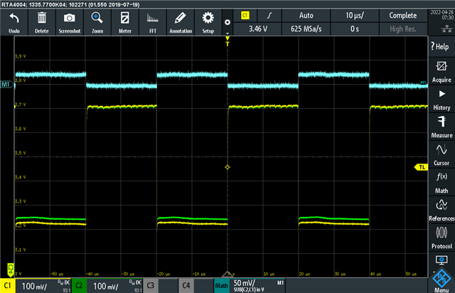
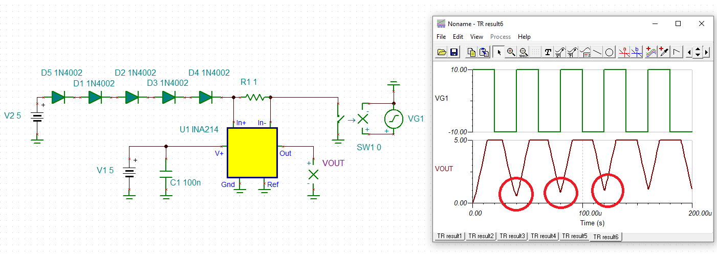
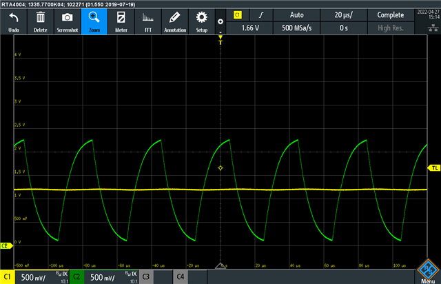
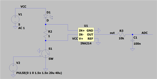
We use the INA214 since several years to measure the current mean of a laser (schematic in picture). The current is a 25kHz square wave.

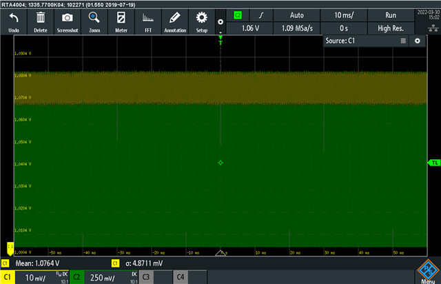
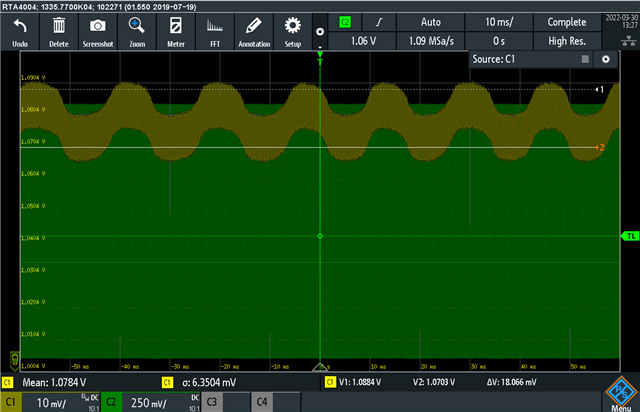
- Everything is working fine, except we found a strange oscillation at the INA214 output, wich does not exist at the input.

- The oscillation frequency goes from about 10kHz down to DC, dependent on the temperature. 

- The oscillation only occurs in every 5th PCB.

- The oscillation triples the standard deviation of the measured current.

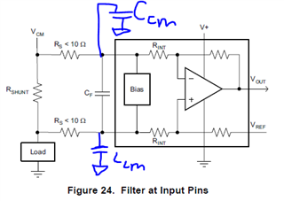
- A 10uF capacitor between IN+ and IN- reduces the oscillation by a factor of 10. 

My question is, how is the oscillation created in the opamp and is there a way to remove it without a layout change?

  • Hi Simon,

    what temperatures are we talking about?

    Is the square wave generation done as shown in the simulation? Is "D1" the laser diode?

    Laser diodes can behave strange sometimes. Have you already scoped the input lines of INA214?

    The output filter has a corner frequency of 160Hz. Where have you observed the 10kHz oscillation? In front of this filter or behind? If in front of, have you used an isolation resistor to isolate the output of INA214 from capacitive loads?

    What about the supply voltage decoupling of "V1" and "U1"?

    Kai

  • Hey Simon,

    Where is the oscillation being observed? At INA214 OUT pin or at ADC input?

    I see two possible root causes here: The ADC load changing over temperature is causing output instability or INA214 coming out of output saturation when S1 switches from OPEN to CLOSED is harder for device when temperature reaches an extreme.

    For the latter cause, the amplifier has certain circuits that can degrade over temperature such as offset chopping circuitry and open loop gain (internal op amp). If the output is saturated and device suddenly comes out of saturation, these circuits have to over correct the non-linear condition of output stage. Thus, the performance of how device comes out of saturation may change over temperature. This is why adding the input cap might have helped. It effectively slows down the input step response from a fast edge to a slower ramp, which contains lesser high-frequency component (energy) and thus makes it easier for device to transition out of saturation and track the input.

    Another way to fix this is to simply provide a small bias voltage to REF pin (~100mV), so that output stage is always in the linear operation range when S1 = OPEN.

    Unfortunately, I am not sure there is a way to remove the oscillation without a layout change. You either need to slow down the step response edge (input capacitor), but this loads down the laser drive, add a small bias voltage to REF pin, or somehow change the load so that output can recover faster such as a small pull down resistance (~10k) or a buffer op amp between CSA and ADC.

  • Thank you Kai,


    - The oscillation frequency comes down to DC at about 29°C. Under 28°C and above 30°C the oscillation is over 1kHz and not critical.

    - A laser driver sets the current with the monitor diode of the laser and than the laser driver modulate the signal with 25kHz. D1 is a laser.

    - The yellow and green traces are the INA214 inputs and the blue trace is the calculated difference voltage.

    - We observed the low frequency (<160Hz) oscillation in the ADC signal at 29°C. At other temperatures the oscillation is observable before the LP filter (because of the higher frequency).

    - The Laser has a 100uF and 100nF capacitor and the INA214 a 100nF capacitor. I tried to decouple the INA214 supply with an additional Ferrite bead, which didn't helped.

  • Thank you Peter,

    - At 29°C the oscillation has a frequency under 160Hz and is observed at the ADC input and the INA214 output. Under 28°C and above 30°C the oscillation has an higher frequency and is just observed at the INA214 output (because of the LP filter). (see my answer to Kai)

    - I tried a 500mV offset at the REF pin (with an unbuffered resistor divider). This didn't help.

    - I tried a 10k ohm pulldown at the INA214 output, which didn't help.

    - I made a measurement without the ADC and LP filter. This didn't help.

     I still dont't understand why the oscillation occurs and just the input capacitor helps to reduce the oscillation.

    As additional infos:

    - The oscillation goes completly away, if the laser current is a DC and not a 25kHz square wave.

    -  I have the measured ADC signal (yellow trace) at 27°C. (The oscillation is not observed after the LP filter because it has a higher frequency):

    and the same measurement with a low frequency oscillation at 29°C:

  • Hi Simon,

    according to the datasheet the bandwidth of INA214 is only 30kHz. But your input signal is a 25kHz square wave with steep edges which contains very high going harmonics. Because of this you massively dynamically overload the INA214:

    simon_ina214.TSC

    The INA214 goes off its linear operation range and begins to behave unlinearily. The dynamic and static saturation effects differ from period to period and what you see at the output after the low pass filtering is just an average voltage which wanders weirdly looking like an oscillation at a lower frequency. This oscillation you observe is just an artefact of the nonlinear operation.

    I think you would need to take a much faster current sense amplifier.

    Kai

  • Hey Simon,

    What is the supply voltage and what is the peak current you are expecting through diode? 

    Why is the DC output voltage different between the two scope shots?

    Do the measurements you get aside from the abnormal oscillations make sense?

    What is the frequency of the output noise on the green channel?

    Is the input voltage noisey? Based upon your first scope shot where you say green and yellow are the INA214 inputs (are these IN+ and IN- with respect to device GND)? Or are these output voltage nodes? 

    Some circuitry in the device could have a clock that is experiencing temperature drift and thus noise can manifest at different temperatures. Either the input cap is helping stabilize something like this inside the device or it is filtering out either differential current or common-mode voltage disturbances above the diode driver. This is why I ask for clarification on the first scope shot.

    Sincerely,

    Peter

  • Thank you very much Kai and Peter, I appreciate your help!

    That's right Kai, the frequency is to high for the INA214. I'm just surprised, that higher frequencies are not simply attenuated from the INA214. Maybe this is actually a problem.

    Figure 6: This picture shows the INA214 output signals, green trace INA214 output, yellow trace low pass filtered INA214 output

    Peter:

    - The supply voltage is 5V, the peak current is about 20mA-22mA.

    - In the two pictures from my privious answer to you (picture at 27°C and 29°C), the yellow trace is the lowpass filtered INA214 output and the green trace is the INA214 output (the green trace is not really usefull because i zoomed out). The yellow trace has an DC offset in the oscilloscope screen, I used that to zoom in further. Unfortunatly you can't compare the DC value of the yellow and green trace in this scope picture. The two DC values are the same in reality. Answered that your question?

    - Yes the measurement makes sense, we measure 11mA mean current, which is about 22mA peak current.

    - The green channel is the output of the INA214. The oscillation frequency changes from 10kHz to DC, temperature dependent.

    - For my feeling the input voltage is not noisy. Yes, in the first picture in my answer to Kai the green and yellow traces are the INA214 IN+ and IN- inputs refered to the device GND. 

    I made another test, I changed the INA214 on a PCB with the oscillation problem through another INA214 and the oscillation disappeared. So I assume the INA214 has something todo with the oscillation.

    At the moment I think the oscillation could come from a modulation of the INA214 input signal (the 25kHz square wave) and some switching circuit in the INA214. Has the INA214 a switching capacitor/chopper circuitry?

    Sincerely,

    Simon

  • Hey Simon,

    Yes there is some chopping circuitry, but I am not sure this is the problem. The output of the device seems to be swinging pretty close to ground and so I always worry about output ground saturation.

    However I believe you are right that this is all to do with the switching on the device. I actually now think this is an AC CMRR problem. Since you first scope shot is of the input voltage, I can see a 450mV square wave input common-mode signal. These fast edges in VCM stress the device CMRR more so because of the higher energy content. It is possible that CMRR can be slightly shifting over temperature and thus showing up as oscillation/ringing some time as temperature changes.

    Maybe try placing an input filter at device as shown below. This may help reduce effect of AC CMRR. Start with 100 Ω input resistors (Rs). For differential input cap (Cf), choose the largest possible value that won't severely impact measurement. Make the common-mode caps (Ccm) = Cdiff/10.

     Best,

    Peter

  • Hi Simon,

    That's right Kai, the frequency is to high for the INA214. I'm just surprised, that higher frequencies are not simply attenuated from the INA214. Maybe this is actually a problem.

    Yes, from my point-of-view the INA214 is hopelessly dynamically overdriven and I would go for a much faster current sense amplifier.

    Kai

  • Thank you very much Peter and Kai,

    you helped me alot.

    I will use an input filter or try some much faster amplifier.

    Sincerely,

    Simon