This thread has been locked.

If you have a related question, please click the "Ask a related question" button in the top right corner. The newly created question will be automatically linked to this question.

LMP2021: Prediction of Ib temperature drift

Part Number: LMP2021
Other Parts Discussed in Thread: OPA387, , TINA-TI

I have a design that includes a high gain, low frequency amplifier for a low level, high impedance source.  The source impedance is 1MOhm and the input level is several microvolts.  The bandwidth of the amplifier can be 1Hz or less as it will be amplifying signals that can be observed in real time. and the gain needs to be at least 150.  Offsets can be trimmed as part of the operating procedure.  So, while a low absolute amplitude of offsets is useful, the important thing is the drift with temperature and the random wander. I am aiming for around 0.1 microvolts per degree temperature sensitivity.

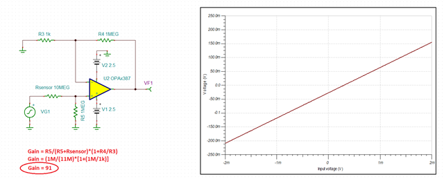
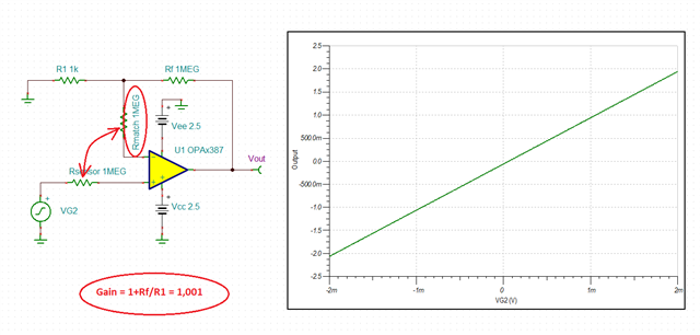
I have been looking at two amplifiers, the LMP2021 and the OPA387.  These have excellent low level offset voltage and drift.  Also, the 1/f noise of the OPA387 should meet my requirements and that of the LMP2021 comes close enough that I may be able to use it.

The problem is understanding the effect of input bias current in these amplifiers.  A drift of 0.1pA per degree into 1MOhm would result in the limit I have set of 0.1 microvolts per degree.  The data-sheets don't give clear information on whether this can be achieved. 

The OPA387 data-sheet suggests the use of lower impedances but this isn't an option.  It also suggests matching the impedances seen by the two inputs.  However this would result in a feedback resistor of 150MOhm for the gain of 150.  Would that achieve the desired result?

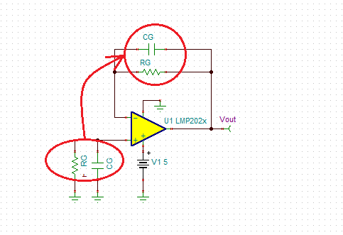
The LMP2021 data-sheet says quite a lot on the matter but isn't clear about how to use the information.  An example is given in Section 8.1.3 for reducing the bias currents for a 1GOhm input resistor in a non-inverting amplifier.  It says, "Figure 41 can be used to extrapolate capacitor values for other sensor resistances. For this purpose, the total impedance seen by the input of the LMP202x needs to be calculated based on Figure 41. By knowing the value of RG, one can calculate the corresponding CG which minimizes the non-inverting input bias current, positive bias current, value."  However, it gives no indication of how to actually do this.  How do I use this figure to extrapolate values for my design?  Also, if a very low bias current is achieved does that imply low drift with temperature?  Section 8.1.4 then tends to contradict the previous section by suggesting that, rather than choosing an optimum value for capacitance, the bigger the better.

Could you please provide some clarification on this.  It these amplifiers are not suitable, can you suggest something better.  I have found amplifiers that have good, low bias current drift with temperature but they have too high a value of 1/f noise.

  • Hello Hugh,

    A low offset voltage and offset drift, or a low IB, does not necessarily means a low IB drift - this is especially true in the case of zero-drift amplifiers like LMP2021 and OPA387.  In order to provide you with a best option, we would need to see your circuit schematic including the resistor values used to gain up the signal.  Also, what is the required temperature range of your application and power supply voltage used?  

  • The design can be flexible to meet the requirement.  As the input sensor needs to feed into a high impedance, I had planned to connect it to the non-inverting input and have a 1MOhm resistor from the non-inverting input to ground to provide a path for bias current (the sensor impedance is higher than 1MOhm and varies with the signal but I can allow for the variation).  The gain would then be as in a standard non-inverting amplifier.  I can choose the other resistors around the amplifier to optimise noise and drift.  As only low frequency operation is required, the 1MOhm resistor on the input could have a capacitor of up to 1uF across it.

    If an inverting configuration would give better results, I can do that with the input being fed through a 1MOhm resistor to the inverting input.  This would then require a feedback resistor of around 150MOhm.  Any resistor connected between the non-inverting input and ground can be chosen to minimise noise and, again, capacitors that limit the bandwidth can be added to the circuit. I have assumed this configuration would give worse results as the bias current on the inverting input would be feeding into much more than 1MOhm.

    I can be flexible with power supply voltage from 2.5V (or +/- 1.25V) to +/- 15V.

    The design is for a laboratory based instrument and the temperature will be room temperature and fairly stable, say between 15 and 25 degrees at any one time as a worst case.  As I mentioned before, day to day variations can be calibrated out by the operator before using the instrument.

    My problem is that it is difficult to design for the high impedances in the circuit as the data sheets give very little information about low frequency current noise and bias current temperature drift.

  • If you perform an initial calibration of the system and need the input offset drift below 0.1uV/C, OPA387 may be a very good choice. But with the input at uV level you probably need a gain of at least 1,000 in order to maximize the output range. Also, I used dual +/-2.5V supplies to avoid need for a level shift.

    You say you "had planned to connect the sensor to the non-inverting input and have a 1MOhm resistor from the non-inverting input to ground to provide a path for bias current (the sensor impedance is higher than 1MOhm)" BUT if you do so your the input will be attenuated by the ratio of 1M/Rsensor - see below.

    I presume the sensor should be able to directly drive a non-inverting input of the amplifier and thus there is no need for another resistor to ground.  Also, in order to minimize the error caused by chopping IB spikes, the input impedances may be matched without the need for 150Mohm feedback resistor - see below.  By doing so, you do not need to worry about IB temperature drift especially if the temperature range is between 15C and 25C. 

    Below I have attached Tina-TI schematic for your convenience.

    Hugh OPA387.TSC

  • Thanks.  There are some useful insights there. 

    I am still not getting something about the bias currents.  My understanding is that in these types of amplifiers the bias currents to the inverting and non-inverting inputs have opposite signs.  This can be seen in the data sheets for the two devices we have been looking at where the offset current is quoted as being twice the bias current.  Therefore the trick of using similar resistors to the two inputs to cancel bias currents doesn't work.  Are you saying then that, rather than cancelling the effect of the bias currents, the similar resistors actually reduce both bias currents and/or make them more stable.

  • In short - yes. The input bias currents in chopper amplifiers do have opposite magnitude at any given instant of time BUT they keep switching back and forth at every clock auto-correction cycle  Thus, the error comes NOT from a DC components of the said currents but only from the mismatch between the positive and negative magnitude of those currents.  For this reason, matching the input impedances cancels error created by the IB's mismatch just as it does in the bipolar input op amps with no IB cancellation.

  • Thanks.  I think that gives me enough to be going on with.  I now need to do some more thinking and perhaps some experimenting.

    It leaves one question open.  In the data sheet for the LMP2021, perhaps for my future reference, how is Figure 41 in Section 8.1.3 to be interpreted and what is it that can be extrapolated from it?

    Update:

    After some further investigation I came upon something that I didn't find in my initial search but seems to address this last question.

    e2e.ti.com/.../inquiry-regarding-lmp2021-cg-equation

  • One could also get around extrapolation of Fig 41 in LMP2021 by matching the input impedances as shown below.