This thread has been locked.

If you have a related question, please click the "Ask a related question" button in the top right corner. The newly created question will be automatically linked to this question.

TLV9002: Can we Connect CT to TLV9002

Part Number: TLV9002
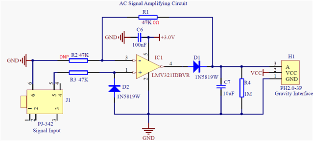
Other Parts Discussed in Thread: CC3220MOD, , TINA-TI, XTR115

Hi,

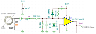
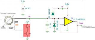
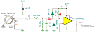
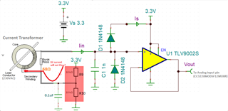
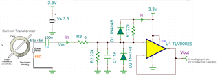
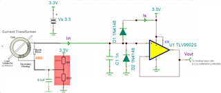
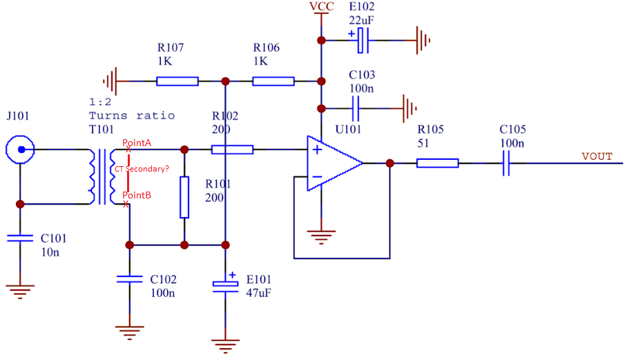
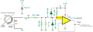
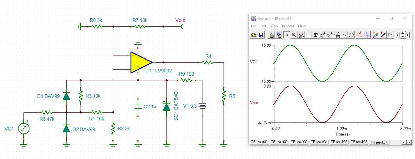
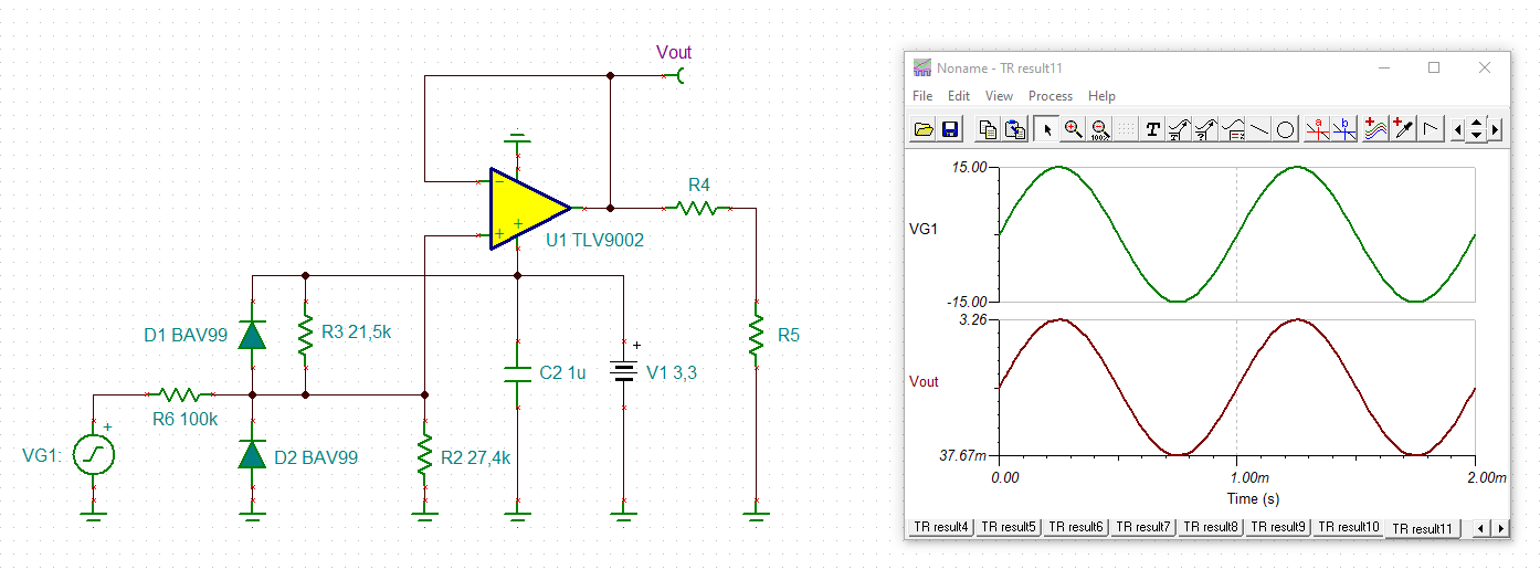
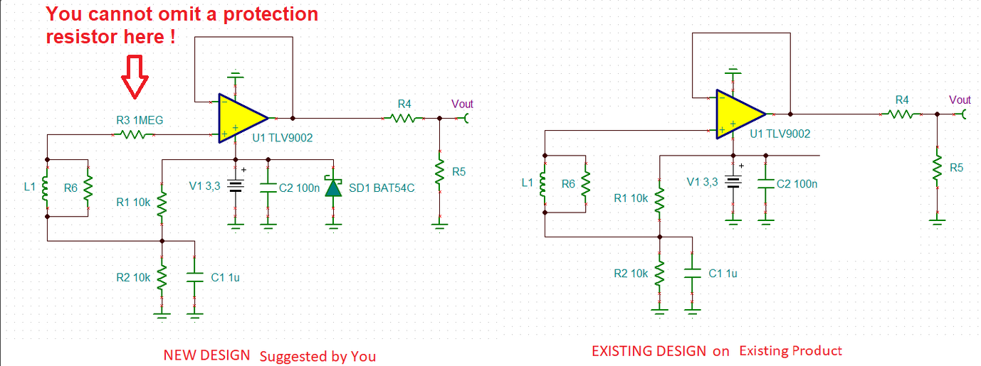
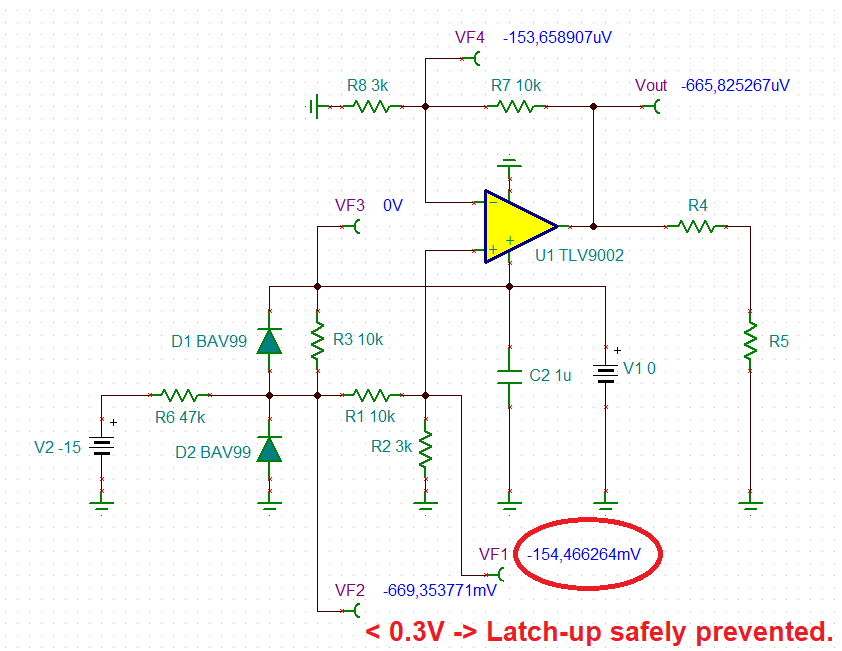
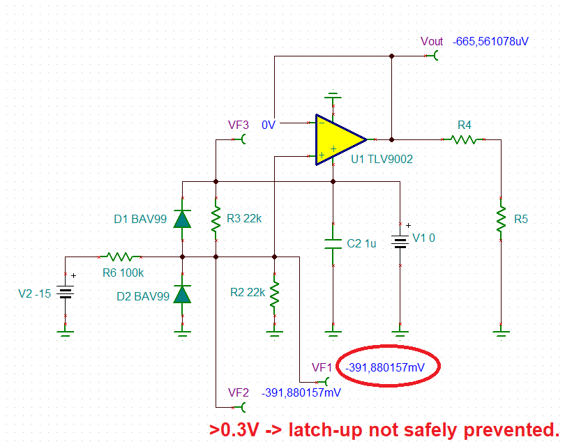
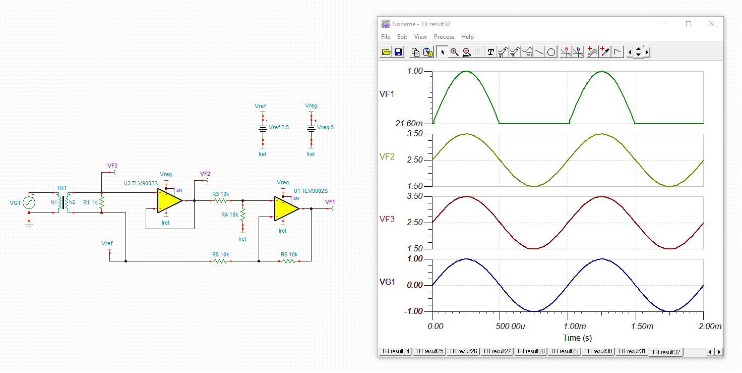
As suggested for the last post from Ron Michallic, below schematic is working fine for the input voltage range from -15V to +15V.

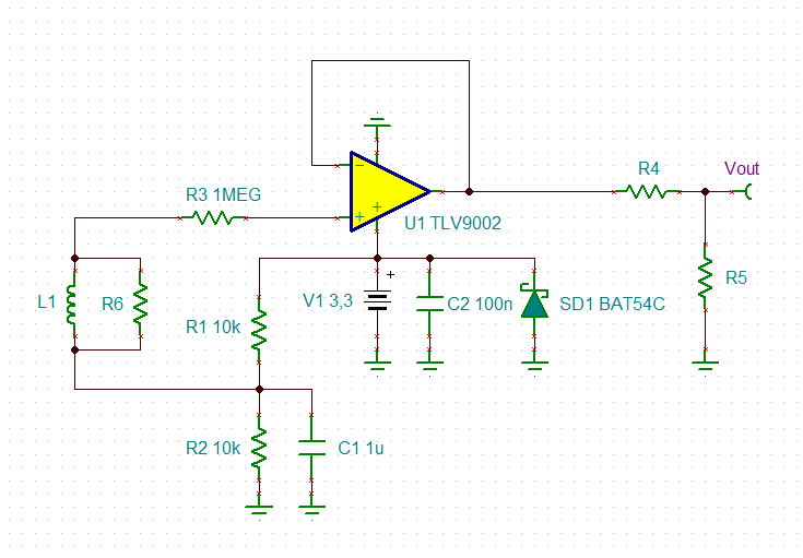
Our doubt is, Can we connect Current transformer for the same schematic as shown below? Any modification required or existing Schematic will works fine? 

Thanks and regards,

Naveen K

  • Hi Naveen,

    this circuit is not so well suited for amplifying a current transformer signal, because the circuit allows the flow of a DC current through the secondary winding of current transformer. This DC current can shift the magnetic properties of core of current transformer. A circuit which prevents the flow of any DC current would be better suited:

    http://www.ko4bb.com/getsimple/index.php?id=isolation-amplifiers

    Another remedy is to use AC coupling by inserting a capacitance between the burden resistance and R3. R3 can also be made smaller, if no signal dampening due to the resistive voltage divider (R1, R2 and R3) is wished.

    Kai

  • Hi Kai,

    Thank you for the information.

    Am having we query, kindly advise individually.

    1. "this circuit is not so well suited for amplifying a current transformer signal", means, Circuit will not works to measure the CT voltage or Circuit will works but circuit will shift the magnetic properties will results wrong CT outputs?

    2. DC current path will be from Voltage divider point to CT secondary through R3 Resistor? Input resistor is too High(100K or 10K) and current will be too small (33uA or 330uA) right? This small current also affecting to CT magnetic properties?

    3."Another remedy", This Schematic will works efficiently? If yes please advise the values for Cin, R3? We can use any value like 22K or 2.2K for R1 and R2 right?


    4. We found this schematic in some forums. This schematic will works efficiently or This circuit also affecting to CT magnetic properties?

    5. We found this schematic in some forums. This schematic will works efficiently or This circuit also affecting to CT magnetic properties?

    6. If we use below Schematic from the suggested link,

    6a. We need additional Transformer T101 to connect with Current transformer J101? or T101 is the Current transformer only and we don't need additional transformer and the circuit just start from point A-B?

    6b. There is no AC coupling capacitor between R101 and R102, How it will avoid DC current flow to CT Secondary? 

    Kindly advise, it will be helpful us to do or to avoid redesign for the existing devices.

    Thanks and regards,

    Naveen K

  • Hi Naveen,

    1. "this circuit is not so well suited for amplifying a current transformer signal", means, Circuit will not works to measure the CT voltage or Circuit will works but circuit will shift the magnetic properties will results wrong CT outputs?

    It will work, but can show errors due to shift of magnetic properties. How much and if at all depends on the current transformer which I do not know.

    2. DC current path will be from Voltage divider point to CT secondary through R3 Resistor? Input resistor is too High(100K or 10K) and current will be too small (33uA or 330uA) right? This small current also affecting to CT magnetic properties?

    From audio transformers it's known that even the very small offset voltage of OPAmp can ruin the performance of transformer. How much and if at all your "small current" is affecting the current transformer depends on your current transformer which I do not know.

    3."Another remedy", This Schematic will works efficiently? If yes please advise the values for Cin, R3? We can use any value like 22K or 2.2K for R1 and R2 right?

    This depends on your needs which I do not know. Assumed R3 is set to zero because you don't want aditional signal dampening, then Cin and the parallel resistance of R1 and R2 form a high pass filter with the corner frequency

    fc = 1 / 2 / Pi / Cin / (R1//R2)

    So, as an example, for Cin = 100nF and R1=R2=22k you will get a corner frequency of 145Hz.

    Decreasing the values of R1 and R2 results in an increase of supply current. But if this doesn't matter, then you can decrease R1 and R2, of course. On the other hand, keeping R1 and R2 big will allow the use of a smaller AC coupling capacitance.

    4. We found this schematic in some forums. This schematic will works efficiently or This circuit also affecting to CT magnetic properties?

    This circuit is nearly identical to the circuit 6b. Yes, it will work. But I recommend a filtering cap in parallel to the lower resistor of voltage divider (R10) to suppress the supply voltage noise which is otherwise amplified together with the wanted signal.

    5. We found this schematic in some forums. This schematic will works efficiently or This circuit also affecting to CT magnetic properties?

    You may have noticed that this circuit again lets a DC current flow through the secondary winding of current transformer which I do not recommend until you have verified that is doesn't degrade the performance of current transformer.

    6a. We need additional Transformer T101 to connect with Current transformer J101? or T101 is the Current transformer only and we don't need additional transformer and the circuit just start from point A-B?

    No additional transformer is needed. Consider the shown transformer as being your current transformer.

    6b. There is no AC coupling capacitor between R101 and R102, How it will avoid DC current flow to CT Secondary?

    Only the very small input bias current of OPAmp will flow through the current transformer which does not harm. But, of course, you can add AC coupling as shown in the upper example, if desired.

    Kai

  • Hi Kai,

    Thank you for the information.

    1. "How much and if at all depends on the current transformer"We using this CT1, and the voltage window will be 0-3V to OPAMP input (We have voltage divider at Opamp Output.  Could you please advise?

    2.a. Compare to circuit 3 & 4, How the circuit is differs each other 

    As you told in 6b, bias current of OPAMP will not harm, so we can neglect it. Only the current from the 3.3V source through R1 & R3 (highlighted  Red line) will causing the harm to CT, right?

    2.b. In this circuit, Current from the 3.3V source through R9 resistor will not causing harm to CT? How this circuit will be safe the CT compare to circuit 2a?

     2.c. In general, We can also use Diode in place of Cin capacitor to block current to CT right?

    3.a. "fc = 1 / 2 / Pi / Cin / (R1//R2)"R1 and R2 not connected in parallel, right?

    3.b. For the above(1) CT1 specification, this schematic will works efficiently right?

    3.c. If we use this circuit, no need level shifter to shift negative voltage, R1 & R2 will do the same here(like R9,R10 on figure 4a), right?

    4.a. "But I recommend a filtering cap in parallel (R10)", Now this circuit also works efficiently? Capacitor 0.1uF will be fine or need higher?

    5. "I do not recommend until you have verified that is doesn't degrade the performance of current transformer", Could you suggest how we can verify? Can we verify by measuring the CT voltage across the Burden resistor(68Ω) on all three different Circuit(say, 3, 4, 5), we should get same voltage, right ?

    6.a. R106 & R107 is the Voltage divider to shift the negative voltage of CT, then What is the purpose of R101 & R102?

    6.b. What is the purpose of R105 & C105?


    Asking many things, we using 2a & 2b in two different devices, Your advise will be very helpful us to take a decisions to change the design as FINAL.

    Thanks and regards,

    Naveen K

  • Hello Naveen, 

    Do you know the expected voltage range at the input of the op amp? 

    All the best,
    Carolina

  • Hi Carolina,

    Voltage range at the Opamp input should be 0-3V, it will be differ from CT to CT. Some CT will provide 0-1V.

    We normally use below spec CT with 26Ω Burden Resistor and Calculated the Vp-p Voltage is,

    Vrms= Primary current range / Secondary turns * Secondary burden resistance
    Vrms= 100A / 2500 * 36ohm = 0.04 * 26ohm = 1.04V
    Vpeak= √2 * Vrms = ±1.47V
    Vpeak-peak= -1.47V to +1.47V = 2.9V

    Thanks and regards,

    Naveen K

  • Hey Naveen, 

    With the voltages you have provided, the values are within the op amp's common mode range.


    As CT limits you simulation-wise, the next step is to test in lab. 

    The evaluation boards can be found on the product page: https://www.ti.com/product/TLV9002#design-development

    All the best,
    Carolina

  • Hi Carolina,

    Thank you for the information and we are expecting some thing else.

    I have shared full scenario in the previous replies to Mr. Kai.

    The thing is, We are already using the Opamps in our devices to measure sensor's output voltage ranges from -15V to +15V.

    Now the requirement came is Current Transformer(CT), can be works in existing circuit or not? or any efficient circuit to measure CT voltage.

    Mr. Kai given some comments on existing circuits that may affect CT magnetic properties and suggested some other circuits. Now am asking few query on the suggested circuits in the last reply to Mr. Kai. So. Kindly advise for my last reply to Mr.Kai, will be helpful us to get more confidence to change/modify our existing designs.

    Thanks and regards,

    Naveen K

  • Hi Kai,

    Am awaiting for your advise too, could you suggest for the below query.

    1. "How much and if at all depends on the current transformer"We using this CT1, and the voltage window will be 0-3V to OPAMP input (We have voltage divider at Opamp Output.  Could you please advise?

    2.a. Compare to circuit 3 & 4, How the circuit is differs each other 

    As you told in 6b, bias current of OPAMP will not harm, so we can neglect it. Only the current from the 3.3V source through R1 & R3 (highlighted  Red line) will causing the harm to CT, right?

    2.b. In this circuit, Current from the 3.3V source through R9 resistor will not causing harm to CT? How this circuit will be safe the CT compare to circuit 2a?

     2.c. In general, We can also use Diode in place of Cin capacitor to block current to CT right?

    3.a. "fc = 1 / 2 / Pi / Cin / (R1//R2)"R1 and R2 not connected in parallel, right?

    3.b. For the above(1) CT1 specification, this schematic will works efficiently right?

    3.c. If we use this circuit, no need level shifter to shift negative voltage, R1 & R2 will do the same here(like R9,R10 on figure 4a), right?

    4.a. "But I recommend a filtering cap in parallel (R10)", Now this circuit also works efficiently? Capacitor 0.1uF will be fine or need higher?

    5. "I do not recommend until you have verified that is doesn't degrade the performance of current transformer", Could you suggest how we can verify? Can we verify by measuring the CT voltage across the Burden resistor(68Ω) on all three different Circuit(say, 3, 4, 5), we should get same voltage, right ?

    6.a. R106 & R107 is the Voltage divider to shift the negative voltage of CT, then What is the purpose of R101 & R102?

    6.b. What is the purpose of R105 & C105?


    Asking many things, we using 2a & 2b in two different devices, Your advise will be very helpful us to take a decisions to change the design as FINAL.

    Thanks and regards,

    Naveen K

  • Hey Naveen, 

    A -15V to +15V circuit is not efficient to measure a +/-1.5V source.

    The circuit should measure the burden resistor voltage with high impedance; the measurement circuit should not send current to the source (CT). 

    • All content and materials on this site are provided "as is". TI and its respective suppliers and providers of content make no representations about the suitability of these materials for any purpose and disclaim all warranties and conditions with regard to these materials, including but not limited to all implied warranties and conditions of merchantability, fitness for a particular purpose, title and non-infringement of any third party intellectual property right. No license, either express or implied, by estoppel or otherwise, is granted by TI. Use of the information on this site may require a license from a third party, or a license from TI.
    • Content on this site may contain or be subject to specific guidelines or limitations on use. All postings and use of the content on this site are subject to the Terms of Use of the site; third parties using this content agree to abide by any limitations or guidelines and to comply with the Terms of Use of this site. TI, its suppliers and providers of content reserve the right to make corrections, deletions, modifications, enhancements, improvements and other changes to the content and materials, its products, programs and services at any time or to move or discontinue any content, products, programs, or services without notice.

     Kai does not work for TI, therefore it is possible that he might not reply. 

    All the best,
    Carolina 

  • Hi Carolina,

    Thank you for the information.

     Current Transformer Specification:

    1. "A -15V to +15V circuit is not efficient to measure a +/-1.5V source" mean, -15V to +15V window & resolution was more compare to +/-1.5V, it may affect on Accuracy, right? So, If we reduce the measuring Window to -3V to +3V will be efficient, right? "current to the source (CT)" could you advice the current Path?

    2.a. Compare to circuit 2a & 2b, How the circuit is differs each other; 

    As told, bias current of OPAMP will not harm, so we can neglect it, right. Only the current from the 3.3V source through R1 & R3 (highlighted  Red line) will causing the harm to CT?

    2.b. In this circuit, Current from the 3.3V source through R9 resistor will not causing harm to CT? How this circuit will be safe the CT compare to circuit 2a?

     2.c. In general, We can also use Diode in place of Cin capacitor to block current to CT right?

    3.c. If we use this circuit, no need level shifter to shift negative voltage, R1 & R2 will do the same here(like R9,R10 on figure 4a), this circuit will be efficient right?

    4.a. "But I recommend a filtering cap in parallel (R10)", Now this circuit also works efficiently? Capacitor 0.1uF will be fine or need higher?

    5. Could you suggest how we can verify DC current can shift the magnetic properties ? Can we verify by measuring the CT voltage across the Burden resistor(68Ω) on all three different Circuit(say, 2a, 2b, 3c), we should get same voltage, right ?

    6.a. R106 & R107 is the Voltage divider to shift the negative voltage of CT, then What is the purpose of R101 & R102?

    6.b. What is the purpose of R105 & C105?


    Asking many things, we using 2a & 2b in two different devices, Your advise will be very helpful us to take a decisions to change/modify the design as FINAL.

    Thanks and regards,

    Naveen K

  • Hi Naveen,

    1. "How much and if at all depends on the current transformer"We using this CT1, and the voltage window will be 0-3V to OPAMP input (We have voltage divider at Opamp Output.  Could you please advise?

    An input voltage window of 0-3V is not a good idea for a single supplied OPAmp. And why do you have a voltage divider at the output of OPAmp?

    As you told in 6b, bias current of OPAMP will not harm, so we can neglect it. Only the current from the 3.3V source through R1 & R3 (highlighted  Red line) will causing the harm to CT, right?

    Yes.

    2.b. In this circuit, Current from the 3.3V source through R9 resistor will not causing harm to CT? How this circuit will be safe the CT compare to circuit 2a?

    How shall any DC current flow through the secondary winding of CT? Only input bias current of OPAmp will flow which is neglectable.

    2.c. In general, We can also use Diode in place of Cin capacitor to block current to CT right?

    No, the diodes are for protection only and play a totally different role compared to Cin.

    3.a. "fc = 1 / 2 / Pi / Cin / (R1//R2)"R1 and R2 not connected in parallel, right?

    Of course not. But for the calculation of corner frequency they appear to be in parallel.

    3.b. For the above(1) CT1 specification, this schematic will works efficiently right?

    Not yet. Some components are missing.

    3.c. If we use this circuit, no need level shifter to shift negative voltage, R1 & R2 will do the same here(like R9,R10 on figure 4a), right?

    Similar.

    4.a. "But I recommend a filtering cap in parallel (R10)", Now this circuit also works efficiently? Capacitor 0.1uF will be fine or need higher?

    There's no simple answer. It depends on how much supply voltage filtering is desired.

    2.c. In general, We can also use Diode in place of Cin capacitor to block current to CT right?

    No. See above.

    5. "I do not recommend until you have verified that is doesn't degrade the performance of current transformer", Could you suggest how we can verify? Can we verify by measuring the CT voltage across the Burden resistor(68Ω) on all three different Circuit(say, 3, 4, 5), we should get same voltage, right ?

    Yes, you could do so. But it's way better to avoid DC currents running into the secondary winding of CT from scratch.

    6.a. R106 & R107 is the Voltage divider to shift the negative voltage of CT, then What is the purpose of R101 & R102?

    Yes. R101 is the load for the CT (in your case the burden resistance) and R102 is a current limiting resistor for protection purpose.

    6.b. What is the purpose of R105 & C105?

    R105 is an isolation resistor for increasing the stability, if a cable or another capacitive load is connected to the output. C105 is a DC blocking capacitor to provide AC coupling.

    We normally use below spec CT with 26Ω Burden Resistor and Calculated the Vp-p Voltage is,

    It's not wise to not use the recommended burden resistance. This can alter the gain factor of CT.

    The thing is, We are already using the Opamps in our devices to measure sensor's output voltage ranges from -15V to +15V.

    It's not wise to use a supply voltge for the OPAmp circuit which is higher than the supply voltage of microcontroller. In the case of identical supply voltages you wouldn't need to care about input voltage protection for the ADC of microcontroller.

    Kai

  • Hi Kai,

    Thank you for the information and appreciate your support.

    1."It's not wise to use a supply voltage for the OPAmp circuit which is higher than the supply voltage of microcontroller. In the case of identical supply voltages you wouldn't need to care about input voltage protection for the ADC of microcontroller." & "why do you have a voltage divider at the output of OPAmp?"

    We use same 3.3V supply for OPAMP & Microcontroller, But Voltage divider at OPAMP output is to limit the Voltage to 1.5V max due to the controller(CC3220MOD) analog pin absolute max rating is 1.6V only. But in some other device with other microcontrollers, we have eliminated the voltage divider due to 3.6V abs max rating.

    "An input voltage window of 0-3V is not a good idea for a single supplied OPAmp", Kindly suggest the input Voltage Window ( Normally the CT output will be, 1Vrms i.e 1.414V peak and -1.414V to +1.414V (2.828V) peak-peak Voltage). Normally we measure peak-peak Voltage.

    2b.How shall any DC current flow through the secondary winding of CT? Current From 3.3V source through R9 resistor not flowing to CT as shown? You mean, due to no ground path from other end of the secondary winding of CT, Current will not flow/affect, right?

    6b. "C105 is a DC blocking capacitor to provide AC coupling." OPAMP will also get affected due to DC current flow from controller?

    Considering all 3 Circuit, Could you suggest to use AC coupling Capacitor at both at Input side(CT output lin) and Output side(OPAMP output Vout) or any one will be sufficient?

    7. Could you suggest, Can we use all 3 common circuits above 6B, to measure the CT voltage (Range: -1.414V to +1,414) as well as Analog Voltage (Range -15 to +15V or 0-10V)? or we need to Modify for CT separately and for Analog Separately? AC Coupling Capacitor will not be affecting to measure Sensors Analog Voltage right?

    I hope, this is the last query and your advise will help us to conclude on the design aspects.

    Thanks and regards,

    Naveen K

  • Naveen,

    I cannot speak for Kai.

    I now understand the use of the voltage divider connected to the amplifier output. Note, a failure in the voltage divider would likely cause damage to the micro. 

    Be mindful of the input and output voltage ranges for the amplifier. The amplifier must have ample output headroom from the rails, else you saturate the output stage. 

    AC coupling the input should be fine.   

    As Caro suggested, testing on an EVM may be most beneficial for your application. 

    Best, 

    Jacob

  • Hi Naveen,

    you could do it this way:

    R1 and R2 provide a pseudo ground at mid-supply. C1 suppresses supply voltage noise and common mode noise being injected from the primary winding of CT to the secondary winding. The Schottky diode absorbs supply current when the TLV9002 isn't powered but the CT is delivering its signal current. The Schottky diode limits the negative going voltage to about -200mV. R3 limits the current unwantedly flowing into the +input of OPAmp when the OPAmp isn't powered but the CT is delivering its signal current. R4 and R5 is your output voltage divider.

    With this scheme AC coupling at the input isn't necessary because of the ultra low input bias current of CMOS OPAmp TLV9002. And at the output AC coupling makes no sense because of the unipolar input voltage range of CC3220MOD.

    Kai

  • Hi Jacob,

    Thank you for the information.

    1. "a failure in the voltage divider would likely cause damage to the micro.", 

    If voltage divider also makes failure, then how we can step down the voltage linearly? To measure the Input Voltage of -15V to +15V we have to use Voltage divider only right? Is there any best way to divide the voltage?

    2. Be mindful of the input and output voltage ranges for the amplifier. The amplifier must have ample output headroom from the rails, else you saturate the output stage.

    For 3.3V supply Voltage, we dividing input voltage to 0-3V from +/-15V & APAMP output also 0-3V. So, we have 0.3V buffer, this headroom not sufficient? Kindly advise how much headroom will be fine?

    Thanks and regards,

    Naveen K

  • Hi Kai,

    Thank you for the information and appreciate your support.

    I hope, L1 is Current transformer secondary and R6 is Burden Resistor, right? 

    Only Diode SD1 will be sufficient to absorbs supply current and limits the negative going voltage? No diodes required on OPAMP IN+?

    This circuit will be efficient to measure both Current transformer voltage and Analog Voltage(+/-15V if we use divider) ? 

    You have suggested everything, only last posted queries was open, Could you please advise for my lastly posted query?

    Thanks and regards,

    Naveen K

  • Hi Naveen,

    I hope, L1 is Current transformer secondary and R6 is Burden Resistor, right? 

    Of course.

    Only Diode SD1 will be sufficient to absorbs supply current and limits the negative going voltage? No diodes required on OPAMP IN+?

    According to the datasheet the TLV9002 has internal protection diodes at the inputs. The 1M should sufficiently limit the input current to prevent damage. Of course, an additional voltage divider at the input could be added as shown below. This would prevent the ESD cells from being turned-on at all. I let the modifications to be done as an excercise for you.

    This circuit will be efficient to measure both Current transformer voltage and Analog Voltage(+/-15V if we use divider) ?

    No, this is a totally different issue, as the current transformer is freely floating but the +/-15V voltage source is not. You could do it this way:

    naveen_tlv9002_1.TSC

    This circuit has the advantage that the +/-15V input voltage can even be applied to the unpowered TLV9002 without causing damage, lock-up or latch-up.

    Kai

  • Hi Kai,

    Thank you for the information.

    1. In our existing device having same circuit, but Diode SD1 not present, remaining things are same. We can continue this/our existing Circuit in one of our device. 

    2.a. Could you please tell us, this circuit will works efficiently and sufficient for the Current Transformer? If yes, We don't know the reason for using D1 and R4 , which is also important or we can eliminate? (No need to multiply the input signal. so, we done, R1=0Ω & R2=DNP).

    2.b. In this circuit 2a, we only get Positive cycle, so to read the Input Voltage of Sensors/CT, Full wave will be the efficient or Halfwave will be the efficient results?

    3. Can we eliminate R1 and only using R2,R3, R6 ? Because you know(shared earlier) this circuit is same as our existing circuit except R1 not present and Diode SD1 not present, Gain not present, remaining things are same. If we can able to remove R1,then we can use our existing circuit/devices without design modifications. Kindly advise. 

    Thanks and regards,

    Naveen K

  • Hi Naveen,

    you are absolutely free to do whatever you want. But I wouldn't do that.

    If the input voltage of OPAmp and the supply voltage of OPAmp come from totally different sources, not only damage of the inputs is an issue but also lock-up or latch-up. In such cases I would always spend some efforts to prevent the OPAmp from receiving insane input signals. Proper lock-up protection can be done by using a diode clamp in combination with a voltage divider and setting a gain to overcome the dampening of voltage divider. A less good way to prevent lock-up is to limit the input current to an as small as possible value when the input voltge leaves the common mode input voltage range or even the supply rails. Whether this method works or not depends on the used OPAmp. It is said that the more modern OPAmps are rather free from going into lock-up because the routing on the die has been optimized. But unless the manufacturer explicitely tells in the datasheet that lock-up isn't a problem when exceeding the common mode input voltage range or even the supply rails, I would be very careful. I have seen many circuits in my career which have shown lock-up when no suited input protection scheme was used.

    On the other hand, if you only want to build a cheap toy instead of a reliable product for the industry and every single cent plays a role, why not simplifying the circuit as much as possible and only caring about preventing damage?

    So, yes, if you need to simplify your circuit and save costs and you can live with the risk of observing lock-down, then remove all the parts you want.

    The same is valid for the last circuit you published here. It's a very low cost and trashy circuit which lots of errors and which I would never use. D2 shall remove the negative going half wave from the input of OPAmp. But as being a 1A Schottky diode it shows lots of temperature dependent leakage current causing a huge error voltage across R3. 10µA gives an error voltage of 10µA x 47k = 0.47V at room temperature. At elevated temperatures the error voltage goes up like a rocket.

    C1 and D7 shall make a half wave rectifier. But again the leakage current of D7 will cause huge errors. And having a 10µ cap at the output of OPAmp can cause stability errors.

    This is a trash circuit I would never use. But if you like trash circuits, then use it Relaxed

    Kai

  • Hi Kai,

    Thank you very much for your advise and well appreciated your support.

    Sorry if am wrongly explained.

    No, we are not designing cheap toy. We need to deliver efficient and quality product to our customers(Industry) and cost is second priority (ofcource cost is important but it will come after the Efficiency and Quality).

    Last Query 2, schematic & brought Board is from DF Robo, we thought it will be efficient. We will skip this design.

    Definitely for New Production, we will modify/change the schematic design with your suggested circuit/components.

    But, most of my cross queries are to do the modifications on existing/older product/boards to work efficiently or else product/board may get wasted.  Could you please help me to bring up the existing board, if possible?

    Can we use Existing Circuit 1a and 1b in our Existing Product/board with some possible modification(like component/value change to utilize on existing boards) or it will wont be possible to bring up to works efficiently? Kindly advise, we will do accordingly.

    1a. 

    1b.

    Thanks and regards,

    Naveen k

  • Hi Naveen,

    you can make the following modifications. But you will do it on your own risk:

    But R3 can definitely not be omitted:

    You can decrease its value a bit, mut you cannot omit it. Otherwise the input of TLV9002 would be unprotected.

    Kai

  • Hi Kai,

    Thank you for your advise and aprreciated your quick response.

    We will try this for existing boards and we will implement rest all in new design.

    1. "The Schottky diode(SD1) absorbs supply current when the TLV9002 isn't powered but the CT is delivering its signal current". only one SD1 will be sufficient to protect all the 3.3V sourced IC's from there respective input signal when there is not powered, right?

    2. "Proper lock-up protection can be done by using a diode clamp in combination with a voltage divider and setting a gain to overcome the dampening of voltage"

    Diode will not works till Voltage at Opamp IN+ exceeds 3.3V (Diode D1 Cathode Voltage) , For IN+= <3.3V(that is for Input=+/-15V) only Voltage Divider will take care and beyond +/-15V diode will add the protection, right?

    Why OPAMP IN+ voltage is too small (0-700mA), we can design till 0-3V and we will have 0.3V buffer, right?

    3. R3 should limit the input current which should be less than 10mA for TLV9002, right?

    Thanks and regards,

    Naveen K

  • Hi Naveen,

    1. "The Schottky diode(SD1) absorbs supply current when the TLV9002 isn't powered but the CT is delivering its signal current". only one SD1 will be sufficient to protect all the 3.3V sourced IC's from there respective input signal when there is not powered, right?

    It's not so simple. When a negative voltage is applied to the input TLV9002, the input voltage is clamped by the internal ESD cell. As consequence an irregular current can flow through the substrate and can turn-on pn-junctions which are never turned-on during normal operation. This can open a current path from the supply voltage pin to the negative going input pin and draw a current from the supply voltage line. Most voltage generators don't like negative going voltages at their output at all and can go into latch-up, if the voltage regulator is turned-on by a rising input voltage while the output voltage is still negative.

    But even with this latch-up preventing Schottky diode the inputs of TLV9002 are not save against too high input currents resulting from a negative going input voltage. Because of that a current limiting resistor at the input of TLV9002 is a must.

    Assume the TLV9002 is unpowered and the CT emits a voltage step of only 1V. Then a current spike of way more than the allowed 10mA is flowing into the TLV9002:

    With a 100k current limiting resistor, on the other hand, the current is limited to about 10µA:

    naveen_tlv9002_2.TSC

    Diode will not works till Voltage at Opamp IN+ exceeds 3.3V (Diode D1 Cathode Voltage) , For IN+= <3.3V(that is for Input=+/-15V) only Voltage Divider will take care and beyond +/-15V diode will add the protection, right?

    Yes. You can run the TINA-TI simulation to see what happens.

    Why OPAMP IN+ voltage is too small (0-700mA), we can design till 0-3V and we will have 0.3V buffer, right?

    I don't understand.

    See the DC potentials at the following nodes:

    naveen_tlv9002_3.TSC

    3. R3 should limit the input current which should be less than 10mA for TLV9002, right?

    Correct. But 10mA only prevents damage of TLV9002. It not necessarily prevents lock-up or latch-up of TLV9002. Because of that the current should be limited to an as small as possible value, way smaller than 10mA. That's why I would suggest a 100k...1M resistor at this place.

    Kai

  • Hi Kai,

    Thank you for the detailed information.

    "Why OPAMP IN+ voltage is too small (0-700mA), we can design till 0-3V and we will have 0.3V buffer, right?"

    "See the DC potentials at the following nodes:"

     My query is related to DC potentials only. As per the Simulator Voltages will be, ,

    For Input V2=0V,     VF2=Vout= 1.66V,  VF1= 0.384V

    For Input V2=15V,   VF2=Vout= 3.27V,  VF1= 0.755V

    For Input V2=-15V,  VF2=Vout= 54mV,  VF1= 12mV

    Any how we have R6 to limit the current even we can use R6=100K, Why we need additional divider Resistor R1 here, we can omit and merge VF1 & VF2,right? Combination of R6=100K,R3=22K, R2=22K voltage Divider and D1-D2 will not be sufficient to protect from Latch up for Input +/-15V? Because, we can input upto 3V to VF1 and still we have 0.3V in buffer on OPAMP input specification, right? Kindly advise.

    Thanks and regards,

    Naveen K

  • Hi Naveen,

    You might also want to read section 2.9 of this appnote:

    8637.snoaa35b.pdf

    Kai

  • Hi Kai,

    Thank you very much for the information and great document, will be helpful.

    Last query that,

    Any advantages to "Shift the negative signal level (waveform )to positive level and reading peak to peak Voltage" compare to "Clamping the negative Voltage and reading only Positive(Only Peak) signal voltage"?\

    Thanks and regards,

    Naveen K

  • Hi Naveen,

    in any case the OPAmp would need to run in its linear range for both methods when you want to get precise resuslts. A clamping of negative half wave outside the common mode input voltage range or even below the negative supply voltage will NOT give precise results.

    But a precision half wave rectifier or a precision full wave rectifier can absolutely make sense.

    Kai

  • Hi Kai,

    Thank you for the information.

    Yes, it's true. But my questions related to efficiency. Mean, If the sine wave positive peak and negative peak is not equal (As shown below waveform) due to nature of the signal or due to noise/interference, if we have the peak-peak voltage(Shifted-Full Wave) we can average both peaks to increase the efficiency with help of reference voltage and in case for Half wave the error rate will be more due to missing of negative peak. My assumption is correct or wrong?

    My one more query is that, Can we measure the 450VAC phase to phase Voltage(Without Neutral) without using transformers, like below assumption circuit? Could you please advise or we need to post with new Case?  

    Thanks and regards,

    Naveen K

  • Hi Naveen,

    usually, the RMS value is calculated when measuring mains voltage. Peak-to-peak measurement can give totally wrong results when the mains voltage is contaminated with noise and harmonics.

    And as I said earlier, your half wave rectification will not give precise results because you not only leave the common mode input voltage range but also the supply voltage range of OPAmp. This circuit is trash.

    Kai

  • Hi Kai,

    Thank you for the information.

    Okay, to maintain OPAMP common mode input Voltage range, we should use Full wave with positive level shift.

    To measure 450VAC voltage- "Peak-to-peak measurement can give totally wrong results" then, how we can measure 450VAC phase-phase voltage? Please advise.

    Thanks and regards,

    Naveen K

  • Hi Naveen,

    there's no simple answer. If the AC voltage is a pure sine, you can do a single wave or double wave rectification with an added low pass filter to get the average. Another approach is to use peak detection.

    If the AC voltage is not a pure sine but is showing harmonics, on the other hand, you should calculate the RMS value. You can do this either by the help of a RMS to DC converter chip or by performing a numerical calculation with a microcontroller. 

    The average of a rectified sine is not identical to its RMS value. They differ by the so called "form factor":

    https://en.wikipedia.org/wiki/Form_factor_(electronics)

    Kai

  • Hi Kai,

    Thank you for the information and Thank you for your support all the time.

    By using above 3phase circuit with Low-pass filter or CT Circuit(with additional Series Resistors), we will measure the peak or p-p voltage and convert peak to rms voltage by Vrms=0.7071*Vp or Vrms=0.35355*Vpp. I hope, it will works fine.

    Thanks and regards,

    Naveen K

  • Hi Naveen, 

    Please let us know if you have any further questions.

    Best,

    Jacob

  • Hi Kai,

    Thank you for the information. It will be very helpful for 4-20mA projects.

    I hope, to measure the CT voltage to calculate the current, below circuit will be sufficient. 

    To convert the same to 4-20mA output need 4-OPAMP+1-XTR115 ?

    We can also connect XTR15 to below circuit? 

    If yes then why the below complex circuit? Mr. Winiston using this complex circuit or above-simple circuit?

    Thanks and regards,

    Naveen K

  • Hi Naveen,

    the link was only given to show you how to design a single supplied precision rectifier in combination with pseudo ground. Nothing less and nothing more Relaxed

    Kai

  • Hi Kai,

    Thank you for the information. it will be very helpful.

    Our circuit is not have Precision rectifier and hope not required. But in which cases Precision rectifier will be required?

    In schematic you have used only one diode instead 2 diodes in the datasheet, so you have designed Half wave precision rectifier, right?

    " /cfs-file/__key/communityserver-discussions-components-files/14/xtr115_5F00_1_5F00_current-Output.TSC "I hope this circuit will be connected to XTR115 Vin to output 4-20mA, right?

    Could you please suggest the Circuit to measure 3-phase(450VAC phase-phase) AC voltage?

    Thanks and regards,

    Naveen K

  • Hi Naveen,

    a standard rectifier or a non-precicion rectifier is used when you only want to remove one half wave of a signal and you don't need any precision, to detect the presence of a signal. for instance. A precision rectifier, on the other hand, is used when you carry out a measurement and you need precise results. I hope you want precise results with your measurement?

    Kai 

  • Hi Kai,

    Yes, We need to measure precise results. Requirement is to monitor the Voltage and current.

    Earlier posted linked Circuit is also a Half wave rectifier, You mean this circuit will give more precise results than our CT-Circuit ? Even we are using amplifier instead normal rectifiers, so, how our circuit will no be precise? Kindly advise, how to proceed to get precise results.

    /cfs-file/__key/communityserver-discussions-components-files/14/xtr115_5F00_1_5F00_current-Output.TSC

    Thanks and regards,

    Naveen K

  • Hi Naveen,

    Even we are using amplifier instead normal rectifiers, so, how our circuit will no be precise?

    A low cost single supply rectifier often runs the OPAmp during more than one half wave outside its linear operating range by driving the inputs out of the common mode input voltage range and/or by driving the output into saturation, or by other words, by pushing the output voltage too close to the negative supply voltage (0V).

    This has two effects: During the "clamped" half wave the signal voltage can show a huge error because the signal voltage is clamped to a saturation voltage, which can differ from OPAmp to OPAmp, from circuit to circuit and which will show a huge temperature drift. This error voltage -which you expect to be zero but is not-  is always added in the rectifier to the "proper" half wave signal and ruins the precision.

    Another effect is that the OPAmp needs time (overload recovery time) to get out of the saturation. So the "proper" half wave signal is affected as well.

    Unwanted error voltage due to saturation of "clamped" half wave together with unwanted turn-on time delay of "proper" half wave forbidd the use of such a low cost single supply rectifier in a precision application. The OPAmp must always run in its linear operating range. Neither the common mode input voltage range must be violated nor the linear output voltage range of OPAmp.

    Kai

  • Hi Kai,

    Thank you for the information.

    You mean,

    1. Our updated  Circuit will be precise, Because we are using Amplifiers with Full wave to measure peak Voltage and we not clamping and inputs with in Common mode range, right?

    2. Half wave Circuit will not be precise due to clamping will exceeds Common mode input range, So circuit will not be precise until OPAMP will have dual supply right?

    3. In our CT Circuit, we noticed in the Simulator that tells Latchup issue when no power, >0.3V will be on the OPAMP input. So we can use protection Diode to clamp the negative voltage when there is no power, right?

    4. How this Circuit more precise than our Circuit? Kindly advise.

    /cfs-file/__key/communityserver-discussions-components-files/14/xtr115_5F00_1_5F00_current-Output.TSC

    Thanks and regards,

    Naveen K

  • Hi Naveen,

    I would like to encurage you to answer your questions by yourself by running my TINA-TI simulations by yourself. TINA-TI is super simple and free. Keep in mind, that I have spent lots of time and energy to develop the above circuits and to derive the transfer function and I'm not willed to spend even more time on a not ending discussion. My time is limited and I don't get any money for this support Relaxed

    Kai

  • Hi Kai,

    First of all Thank you very much for your Support and time, we'll Appreciated Pray

    I agree, we spend more time, but Given Information will be very helpful. Appreciate your Patience.

    Thanks and Regards,

    Naveen K

  • Hi Jacob,

    Thank you for your support and we'll appreciated.

    Given Information will be very useful.

    Thanks and Regards 

    Naveen K