This thread has been locked.

If you have a related question, please click the "Ask a related question" button in the top right corner. The newly created question will be automatically linked to this question.

JFE150: JFE150 LN preamplifier saturation

Part Number: JFE150
Other Parts Discussed in Thread: LMH6624, OPA202, TINA-TI, OPA354

Hello everyone,

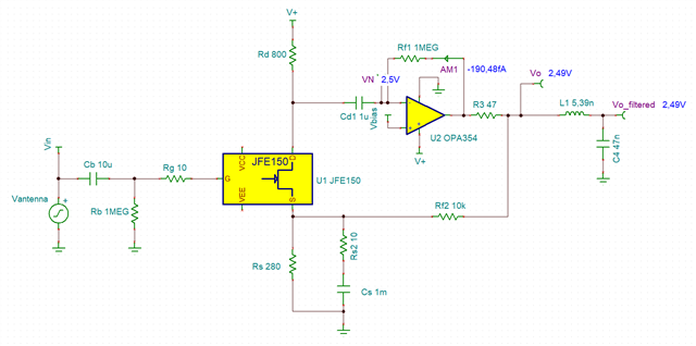
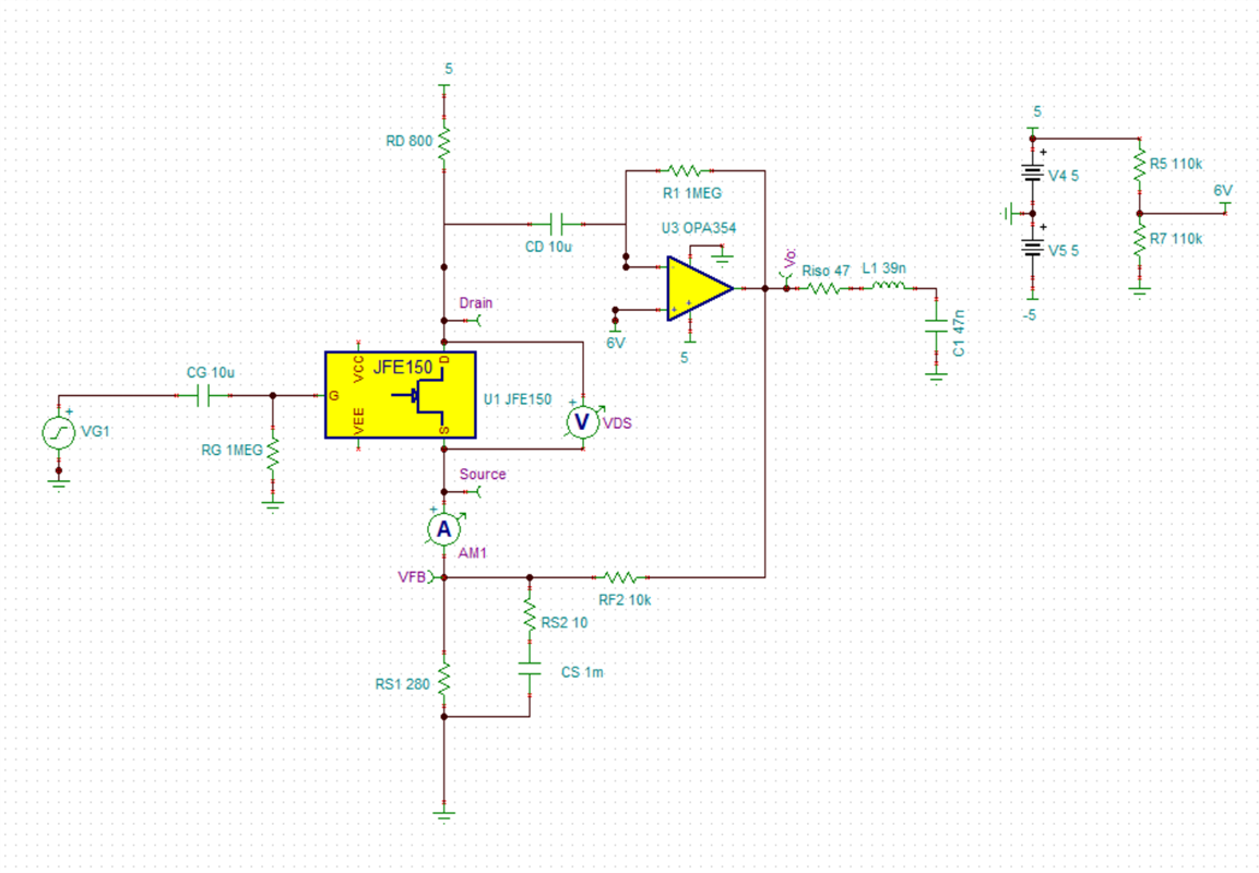
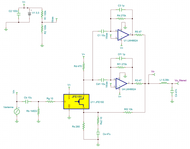
I am using the JFE150 transistor to develop a low noise transconductance preamplifier. The input of this circuit is an antenna made out of a parallel LC circuit. I want to measure the voltage of the LC.

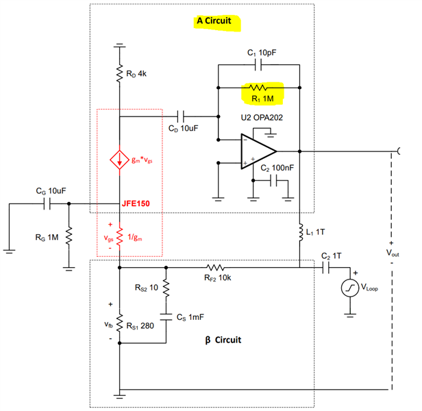
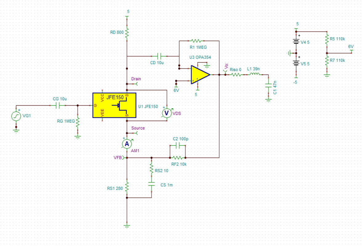
I inspired myself from the JFE150's circuit in datasheet and application note, but as my requirements are a little bit different, I changed the values of some components

  • My frequency range is hundreds of kHz so I changed the OPA202 for an LMH6624 with a bigger GBW
  • I work with a single 3.3V supply and changed Rd from 4k to 470, otherwise Rd would have restricted current to drain
  • I changed Cs to 47uF
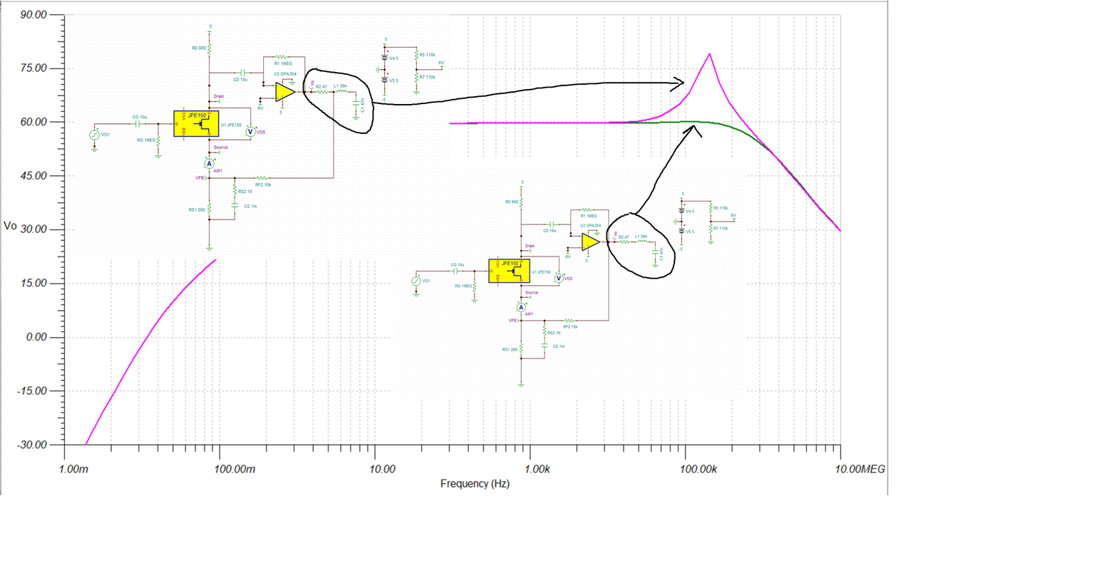
  • I changed the values of feedback network to increase cutoff frequency
  • I put two LMH6624 in parallel to increase SNR to 3dB
  • I added an LC filter at the output

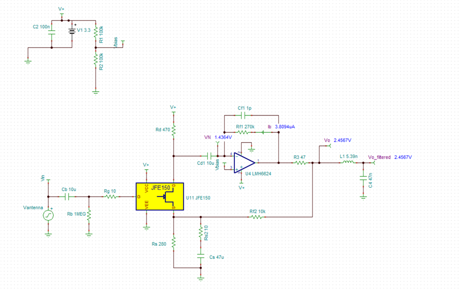
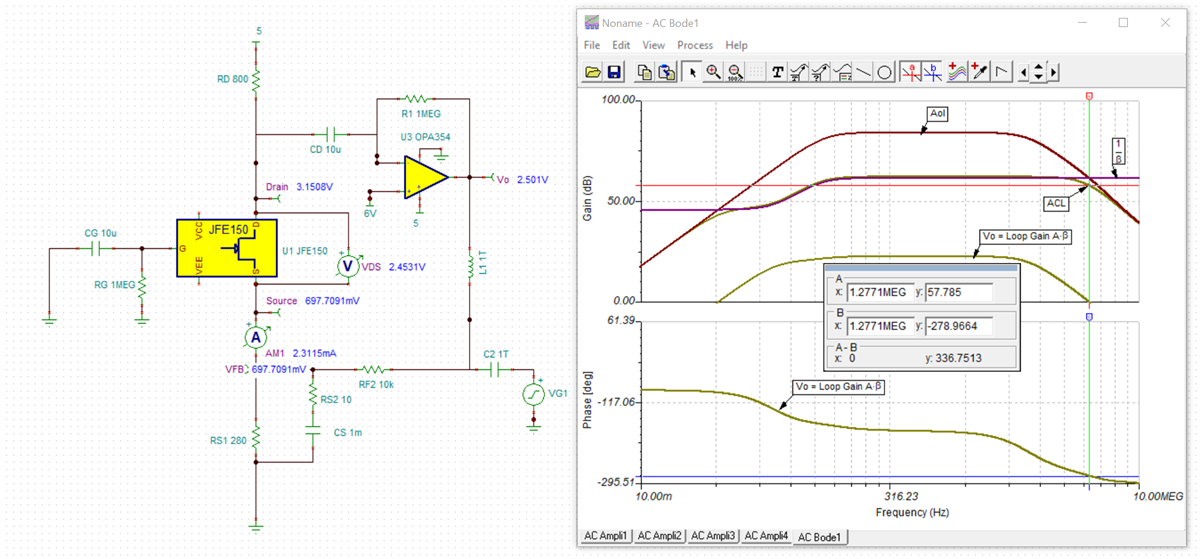
We have the following schematic:

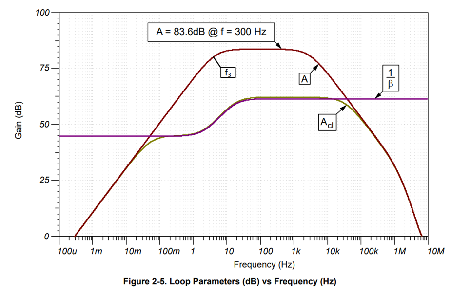
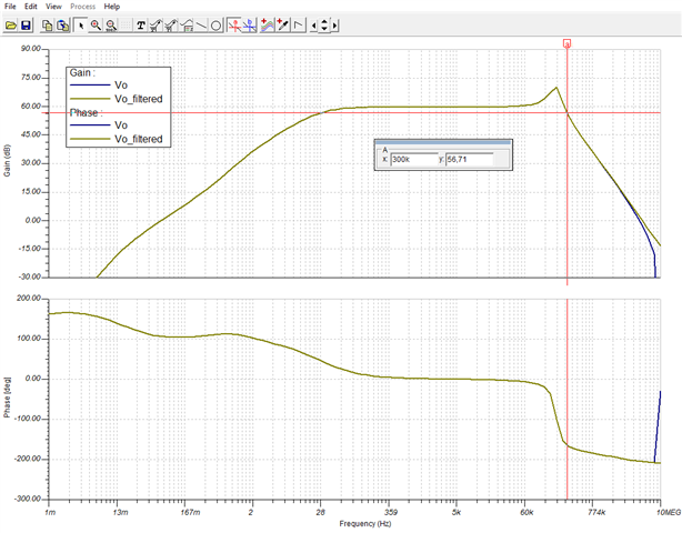
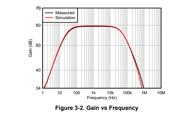
With TINA-TI, the gain is approximately 55-60 dB in my working frequency, which is very good (in simulation)

But as theory and praxis always dance together in a strange way and hide some surprises which makes our days of work sometimes very fun, I had a different behavior on my physical board.

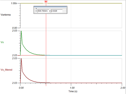
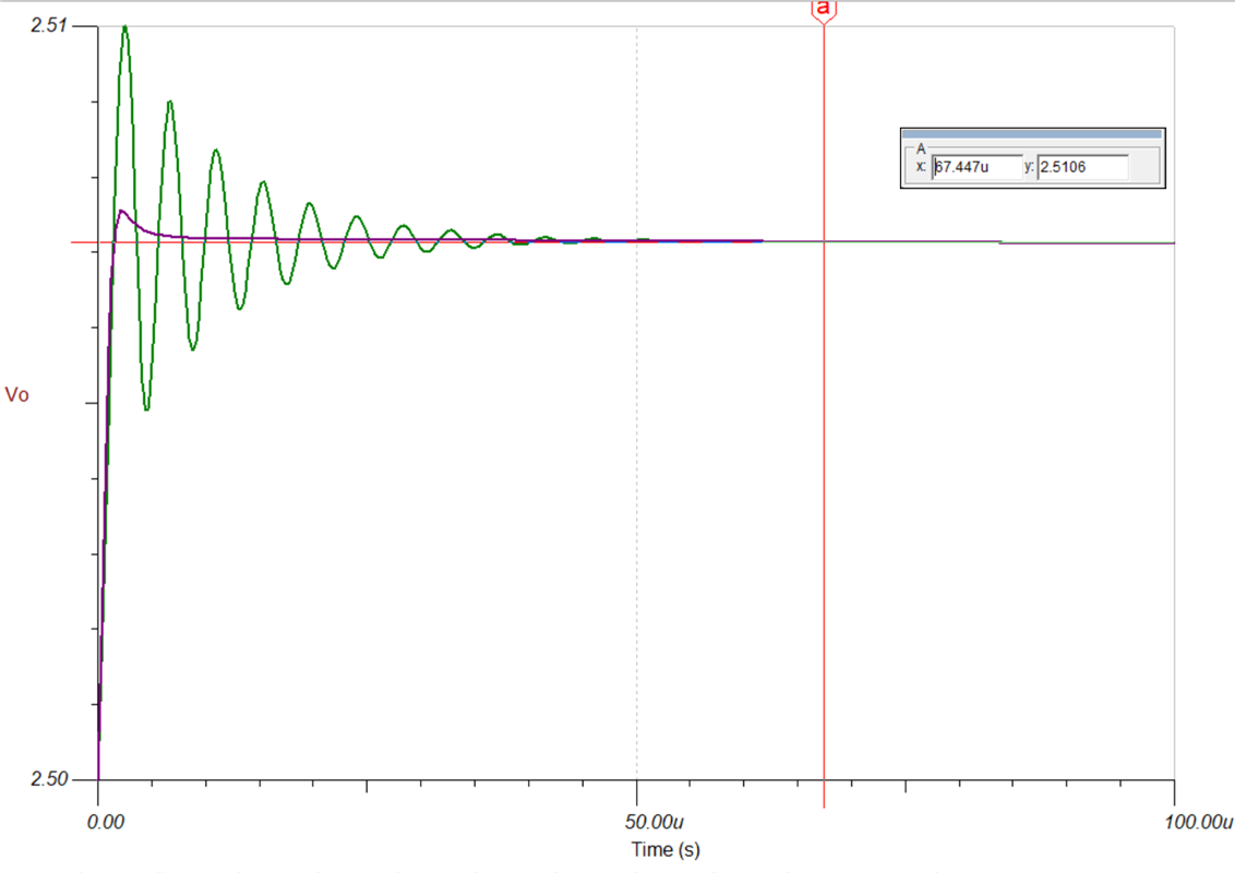
As I put the power on, output increase slowly (approx 2-3 seconds) and stays at 2.55 volts. Voltages are:

  • Vout = 2.55V
  • Voltage on drain is 3.3V
  • Vfb = 2.55V, like Vout
  • Vbias = 1.3V

I tried the circuit with one LMH6624, then with open loop, no change. Behavior stays as described below on the oscilloscope measure:

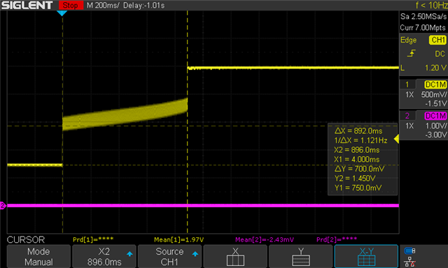
0V (gnd) is at the pink line. First there is a jump of 0.7V, then a sawtooth signal (middle part), then signal jumps again of 0.7V and stays at 2.55V.

  • Does this behavior comes from the clamping diods? I connected VCH and VCL
  • Should I work with dual supply (+/-) instead of single supply?
  • Is there something I didn't see?

Any recommendation, help is welcome.

Thank you very much
Jeremie

  • Hi Jeremie,

    can you share your TSC-file?

    Not looking deeper into your circuit right now, have you considered that JFETs come with huge manufacturing tolerances? Think of the gate source cutoff voltage and the IDSS.

    Kai

  • Hi Kai, thank you for your reply, I didn't considered the gate source cutoff voltage and IDSS, I will take a look

    My TSC file:Analog_signal_processing_chain_LNA_parallel_JFET_LMH6624.TSC

    Best Regards,
    Jeremie

  • Jeremie,

    I wrote an Application Report on this circuit to help guide the conversation. The Application Report can be found here:

    https://www.ti.com/lit/an/slpa018/slpa018.pdf?ts=1652213404751

    Below I have screen captures from my Application Report. 

    I have a couple concerns to address with the circuit. The first concern is that the feedforward gain A needs to be sufficiently larger than the beta network. In my design I had to use a 1Mohm feedback resistor around the amplifier that forms the transimpedance section of the circuit as seen below. 

    Breaking the loop as shown above with components L1 and C2 I plot the A circuit, 1/beta and the closed loop gain Acl vs Frequency as shown below:

    We want the closed loop gain to follow the 1/beta curve that comes from the 10k and 10 ohm resistor. The closed loop gain is 10k/10+1 =1001 or approximately 60dB. 

    In order to achieve this result, the A circuit needs sufficient transimpedance gain using the 1Mohm feedback resistor. The upper closed loop cutoff frequency is determined by the intersection of A and 1/B. This is graphically seen in Figure 2-5 above. With such a large feedback resistor it is important for the ib on RF error to remain small in order to ensure an accurate DC Vbias point for the output of the amplifier. The LMH6624 is a high speed device with large ib in the uA range.

    I did notice that the minimum supply of the LMH6624 is 5V on a single supply. In order to help you find an appropriate amplifier I have a few questions:

    1) Is the minimum supply 3.3V or can this be increased?

    2) What closed loop bandwidth does your application require?

    Best Regards,

    Chris Featherstone

  • Jeremie,

    I simplified your circuit for analysis purpose to just one amplifier. I see that the simulation output voltage is 2.45V due to the Ib on RF1 error plus the Vbias and Vos. In order to reduce this error, a much lower Ib device would be needed. The LMH 6624 appears to be railed out. The no load output swing from the supply is 1.25V down from 3.3V. The minimum supply voltage needs to be 5V. 

    Changing the supply on the op amp to 5V and applying a step signal while monitoring the output voltage I see that it should take roughly 1/2 seconds to settle the output DC voltage. This is due to the time constant between the 10uF cap CD1 and RF in the feedback of the op amp. 

    Best Regards,

    Chris Featherstone

  • Hi Jeremie,

    like Chris already mentioned, your supply voltage are way too small. The original circuit runs with 12V. Why are you using 3.3V? The LMH6624 needs a minimum supply voltage of 4.5V.

    The JFET also runs with a way too small supply voltage. Keep in mind that the gate source cutoff voltage and IDSS can widely vary from part to part. But with such a small supply voltage you don't have any headroom to compensate for any manufacturing tolerances of JFET.

    So my suggestions is: Divide and conquer -> Try to make your circuit run with a proper supply voltage of 12V first. Then, if everything works properly, try to decrease the supply voltage, if necessary at all.

    There's one more issue: You say that you have a LC parallel circuit at the input. But your simulation runs with an ideal voltage source having zero source impedance. This is not the same and can have a considerable impact on the stability of your circuit.

    Kai

  • Hi Kai and Chris, thank you very much for your help and well detailed explanations.

    Indeed, I made an error with minimum supply voltage on LMH6624, I wanted to avoid another DC-DC converter because my power supply comes from a small 3V battery. But I guess I will have to change my plans. I will do it again with a +5V (or +12V) and increase Rd back to 4k

    I work on the 400 kHz, +/- 100 Hz frequency range. 400 kHz may be changed to a value between 300 kHz and 500 kHz

    Chris, when you mention a much lower Ib device, do you mean increase the Rb1 to reduce Ib? It will indeed reduce my cutoff frequency, but as you explained, to be a good transimpedance amplifier, Rf needs to be bigger.

    Kai, I didn't made a proper analysis of the output impedance of the LC resonator and the impact it may have on the JFET + operational amplifier circuit. First I will apply all your recommendations about power supply and resistance value. I hope the LC impedance won't be of too much trouble, if it does, then I will deal with it :)

    Jeremie

  • Hey Jeremie,

    In my simulation above you will see the current meter I labeled Ib in the feedback path of the LMH6624 that is in series with the resistor RF1 = 270k. Due to the large Ib or bias current on the inputs of the LMH6624, you will observe a large DC error at the output. This is due to the Ib on R voltage error that is developed. The output voltage should be much closer to the Vbias point ideally. However due to the large Ib on R error, the output voltage is 2.45V as seen above. The larger you make that resistor (RF1) the more error you will have. However you need to increase resistor RF1 in order to have a large feed-forward transimpedance gain. 

    Ideally the amplifier would be a CMOS or JFET input stage with low input bias current Ib.

    The Ib for the LMH6624 is in the uA range. 

    Best Regards,

    Chris Featherstone 

  • Hey Jeremie,

    Let me know what you think of this design (Tina attached at the bottom).  I put in the OPA354 that has much lower Ib in the pA range. It can be any similar amplifier but this is just an example. 

    You can see below that I have the JFE150 biased with 2.45V of VDS and an IDS current of 2.3mA. The closed loop gain is 1.27MHz at the -3dB point or where A and 1/beta intersect. The phase margin is 98.97degrees. The closed loop gain can be controlled by placing a capacitor in the feedback of the OPA354 in order to cut the bandwidth of the feed-foward gain A such that A and 1/beta intersect sooner.

    2376.JFE150EVM Gain of 1000 Freq Analysis.TSC

  • I forgot to change the labels for the Vbias point but the circuit still works correctly in the sim. They should be labeled 2.5 as shown below.  

  • Hi Jeremie,

    what are L and C of your LC resonator?

    Kai

  • Hi Chris, thank you again for those helpful advices. I tried your circuit on TINA-TI with the OPA354 and it seems indeed much better for my application.

    I tried it on the "normal" circuit as well as on the T-modell circuit. The bandwith is good, I wanted to reduce gain in lower frequencies so I reduced Cd1 from 10uF to 1uF.

    The value of Ib is now of some fA, so way much less than the previous layout. Output is almost at Vbias, which is perfect:

    There is something I don't understand between the two circuits ("normal" and T model). With T model, we have a flat Acl gain on the working frequencies, but on the "normal" circuit, with input coming from Vin, it creates a different gain bode plot, with a pole in the area of 200 kHz and a bigger phase shift.

    "Normal" circuit bode plot:

    Is the T model the best way to analyze a closed loop circuit, phase and gain, on TINA-TI?

    Another question about the T model, I discovered a difference with the example schematic on JFE150's datasheet on the input side: Rg is on the T model is parallel and the original Rg of 10 Ohms disappears. Is it on purpose? Does it changes something?  

    I also discovered that the 47 Ohms output resistances create a quite huge gain loss (approx 51 dB with it, approx 60 dB without). I will have to check if I keep the parallel opa layout or do it with one only.

    Best regards
    Jeremie

  • Hi Kai,

    Currently, the LC circuit is calibrated to resonate at 300 kHz approx. C is a 3.3 nF film capacitor, L is approx of 85 uH if I am not making any mistake. L has a ferrite core to improve its magnetic permeability.

    Is it possible to simulate the physical/electric behavior of an LC resonator with TINA-TI? And therefore do a better impedance analysis for the impedance matching with JFE150?

    Best regards,

    Jeremie

  • Jeremie,

    I am able to tame the gain peaking by moving the Riso resistor out of the feedback path as shown below. 

    Placing the Riso resistor outside of the loop as shown below I am able to tame the ringing on the output. You can see this with the step response below. 

    I am looking into breaking the loop method with this setup. In the meantime it does appear to be stable with the isolation resistor. 

    Best Regards, 

    Chris Featherstone

  • Jeremie,

    Regarding the 10 ohm RG resistor in the datasheet. I have not used this resistor even in my EVM of this circuit. 

    https://www.ti.com/lit/ug/slpu009/slpu009.pdf?ts=1652390648296&ref_url=https%253A%252F%252Fwww.ti.com%252Ftool%252FJFE150EVM

    I obtained the same result in my real measurement vs Tina simulation:

    Best Regards, 

    Chris Featherstone

  • Jeremie,

    One other method you can use to tame the peaking and ringing is to place a feedback capacitor in the beta network as shown below:

    Best Regards,

    Chris Featherstone