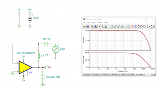
Dear TI members,
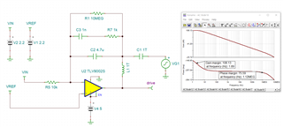
I did simulation with TINA for TLV9002 voltage follower but, the result of AC transfer characteristic analysis is wrong.
could you review my simulation setting or circuits ?
Best regards,
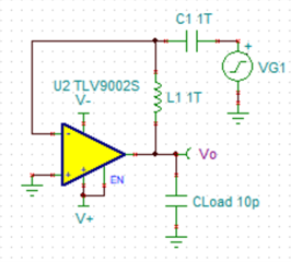
Dear TI members,
I did simulation with TINA for TLV9002 voltage follower but, the result of AC transfer characteristic analysis is wrong.
could you review my simulation setting or circuits ?
Best regards,