This thread has been locked.

If you have a related question, please click the "Ask a related question" button in the top right corner. The newly created question will be automatically linked to this question.

OPA552: Stability Issues with Capacitive loads

Part Number: OPA552
Other Parts Discussed in Thread: OPA551, TINA-TI

Hi team,

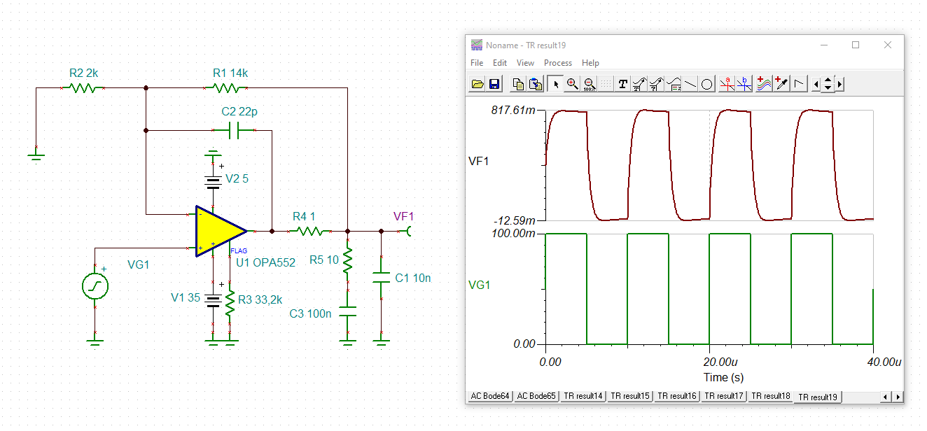
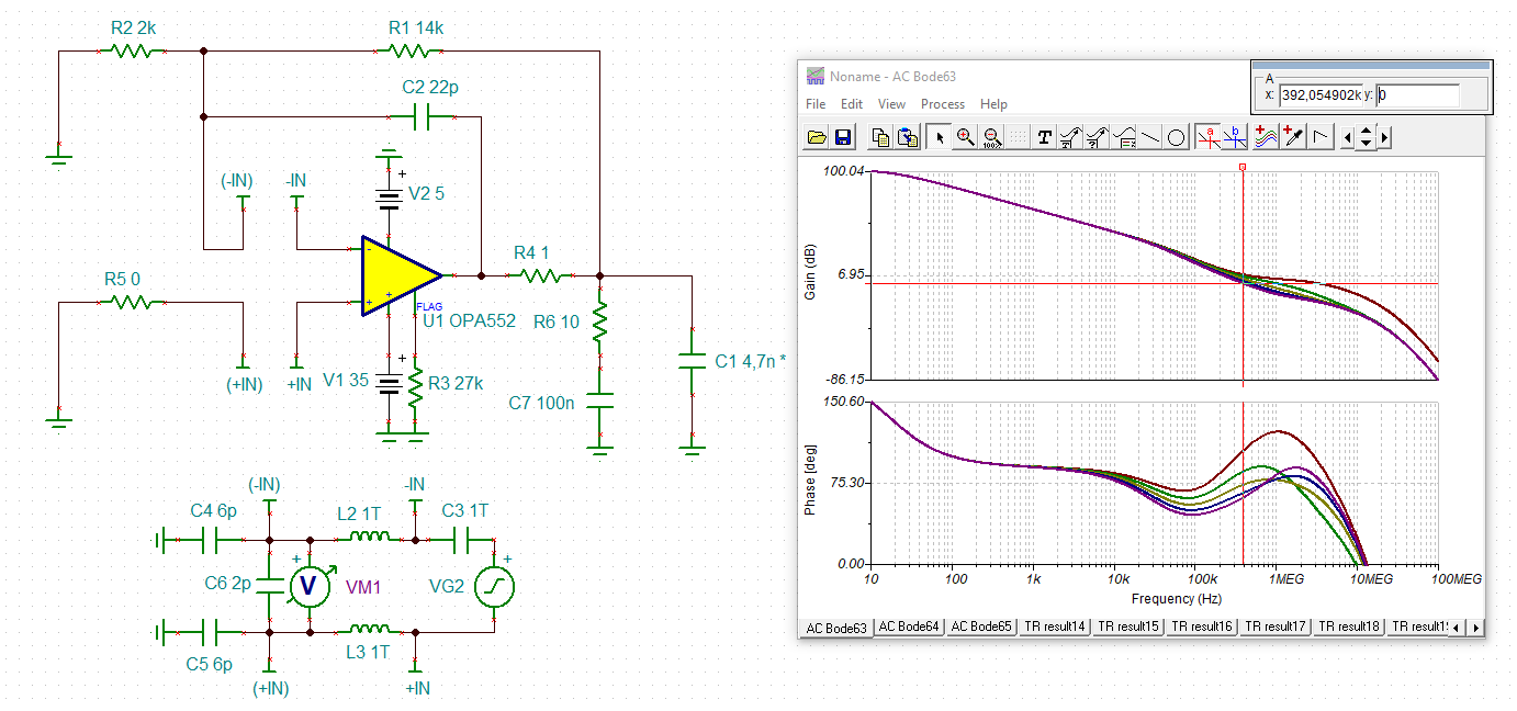
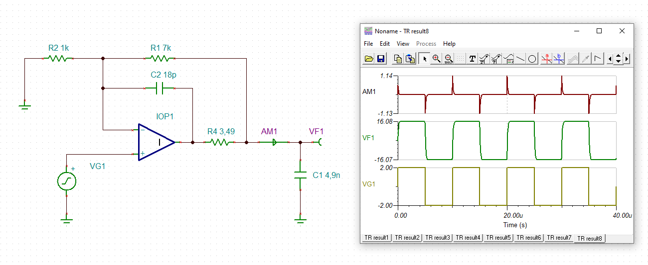
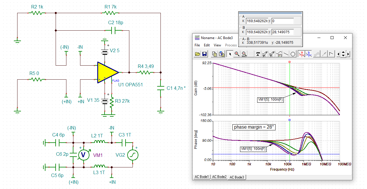
We are using the OPAMP OPA552 in our design as a non-inverting amplifier with Gain8 as shown in figure 1.

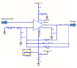
                     Figure 1: Amplifier Circuit


We are seeing more stability problems with this OPAMP. The details are mentioned below,

- The input of the Amp. is driven with 5V, 100KHz square waveform
- The output of the Amp. is connected to capacitive loads (4.7nF used here)
- We are seeing the oscillation as shown in Figure 2
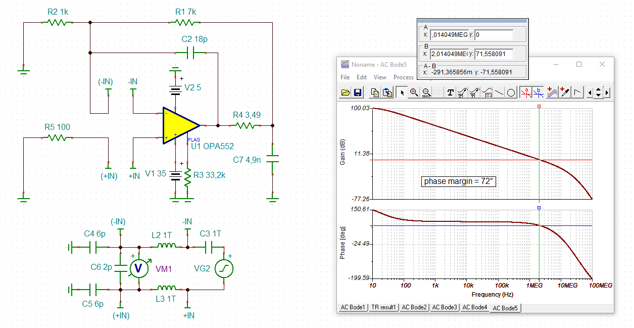
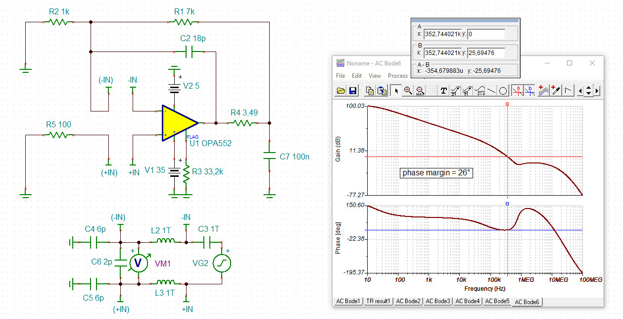
Note : This just an example. We have tried with different frequencies & different capacitive loads, still stability problem is there.

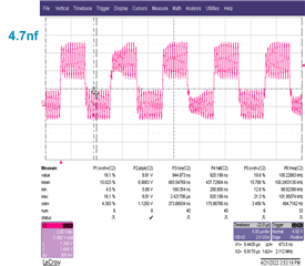
                    Figure 2: Stability Issues

We need your inputs in how to deal with this problem.

Regards,

Ahamed Faize

  • What is the value of R107? Direct cap loads are usually problem, looks like you have started with the imbedded integrator approach, but maybe the values just need to be adjusted. C81 and R107 would be that adjustment. Eventually, you would want to run a LG phase margin sim. Lots of material out there on that, but here is one I had done, 

    https://www.planetanalog.com/stability-issues-for-high-speed-amplifiers-introductory-background-and-improved-analysis-insight-5/

  • Hi Ahmed,

    can you tell more about your application?

    What capacitance range do you want to connect to the output? How is the capacitance connected to the output? Via a cable?

    What is you maximum signal frequency? What shape? What amplitude?

    What resistive load is connected to the output?

    What exactly is connected to the +input? Is there a low pass filter?

    You say your gain is 8V/V and your input signal is 5V. But 8 x 5V = 40V and your supply voltage is only 35V?

    Kai

  • Hi Ahmed,

    Some of our team members are out of office, but you should expect a response within this week.  

    Meanwhile, kindly provide the details for the impedance/capacitive load at the OPA552 output, the input signal frequency/amplitude and circuit details, so we can provide a detailed stability analysis.  As Kai has mentioned, clarify, if the input voltage amplitude is expected at 5V, and the circuit is configured on a gain of +8V/V, with supply rails +35V and -5V, the amplifier output will be out of range.

    Thank you and Regards,

    Luis

  • Hi Michael,

    Thanks for the link. I will check that.

    R107 is 1E.

    Regards,

    Ahamed Faize

  • Hi Kai & Luis,

    Thanks for analyzing the circuit specs. Here are the info that you have asked

    1) What capacitance range do you want to connect to the output? How is the capacitance connected to the output? Via a cable?

    Faize: The capacitance range is 10pF to 100nF. It will be connected through ~10cm female to female jumper cable. 

    2) What is your maximum signal frequency? What shape? What amplitude?

    Faize: Max. signal frequency is 100KHz, square wave. Amplitude can be anything between 0 to 32V

    3) What resistive load is connected to the output?

    Faize: As of now no resistive loads are connected. In later stages, we may use 100mA resistive load (max)

    4) What exactly is connected to the +input? Is there a low pass filter?

    Faize: Input is driven from DAC (DAC7822IRTAT). The low pass filter option is there at the input. (but not used)

    5) You say your gain is 8V/V and your input signal is 5V. But 8 x 5V = 40V and your supply voltage is only 35V?

    Faize: Sorry for the wrong info. The output is 5V & the input is 5V/8.

    Hope I have answered your queries.

    Regards,

    Ahamed Faize

  • Hi Ahamed,

    it's difficult to stabilize the circuit when 100kHz square wave performance is wished. I would give this circuit a try:

    ahamed_opa552_1.TSC

    ahamed_opa552.TSC

    Kai

  • Hi Kai,

    Appreciate you for the simulations. We will look into this.

  • Hi Kai,

    I am colleague of Ahamed Faize. We shall try this circuit as Faize already acknowledged. Meanwhile can you please address my 2 questions : 

    1. Why do you say that it's difficult to stabilize the circuit when 100kHz square wave performance is wished.

    2. What is the theory behind adding RC network at the output?

    Regards,

    Vijetha HN

  • Hi Vijetha,

    1. Why do you say that it's difficult to stabilize the circuit when 100kHz square wave performance is wished.

    For better stability C2 and R4 (in my simulation) would have to be increased, R4 to better isolate the output of OPAmp from the huge capacitive load (C1) and C2 to provide more phase lead compensation. But both results in a decrease of corner frequencies of low pass filters formed by R1 / C2 and R4 / C1.

    2. What is the theory behind adding RC network at the output?

    I use the snubber method to resistively load down the output of amplifier for the critical high frequencies where instability occurs. This results in a snubbing down of the amplifier’s gain and shifts the 0dB point to frequencies where the phase margin is looking better. And the series capacitance is simply used to decrease the loading at lower frequencies.

    The snubber was determined here by trial and error, or better say, by my experience Relaxed

    Of course, the snubber method has always the disadvantage of increasing the load at the output of OPAmp.

    Kai

  • For better stability C2 and R4 (in my simulation) would have to be increased, R4 to better isolate the output of OPAmp from the huge capacitive load (C1) and C2 to provide more phase lead compensation. But both results in a decrease of corner frequencies of low pass filters formed by R1 / C2 and R4 / C1.

    Hi Kai, Yes we are using some formulae to reach suitable values for C2 and R4 such that : There should not be any instability oscillations + 100KHz should be scheivable.

    We used foirmulae as : 

    R4 = (R2*R0)/R1. Where R2 = 1K, R1 = 7K and R0 is the output load resistance of OPA552 (25 OHM).

    C2 = (R4+R0)*Cl/R1. Where Cl = Total Load capacitance (considered 4.7nF + ESD diode capacitance which is 0.2nF and it is not show in the schematics we shared).

    With these calculations, we selected R4 = 3.49 OHM and C2 = 18pF

    With these values of R4 and C2, we do not see any instability oscillations. But one issue is : we have 2 seperate sections of this circuit. In one section we do not see any oscillations using these values (confirmed by testing 10 times) and in another section it showed instability once out of 10 times! That is bothering us. We are working on different ESD diode and re calculating to test again.

    Just to avoid all the calculations, trial/error methods, I wanted to confirm : Do you suggest alternate OPAMP (same footprint is preferred) that has very good stabilty supporting minimum 1MHz BW at Gain of 8 (in other words 8MHz at unity Gain)? Also 32V, 150mA need to be supported.

  • Hi Vijetha,

    R4 = (R2*R0)/R1. Where R2 = 1K, R1 = 7K and R0 is the output load resistance of OPA552 (25 OHM).

    C2 = (R4+R0)*Cl/R1. Where Cl = Total Load capacitance (considered 4.7nF + ESD diode capacitance which is 0.2nF and it is not show in the schematics we shared).

    With these calculations, we selected R4 = 3.49 OHM and C2 = 18pF.

    Then why did you show a different circuit in the first post?

    The new circuit would be stable with a load capacitance of 4.9nF:

    But not with a load capacitance of 100nF:

    There are two issues:

    1. The dual feedback method only works stably for a limited load capacitance range.

    2. Your circuit suffers from the huge load capacitance. Keep in mind that 100nF presents an impedance of 16R at 100kHz and 1R6 at 1MHz where the harmonics of 100kHz square wave can be found. So the OPA552 sees a short-circuit at its output. This might be the reason for your observed "instability".

    Kai

  • Then why did you show a different circuit in the first post?

    The circuit that was posted earlier is actually present in the design and this experiment was done just couple of days ago and hence the new values. 

    Anyways, thank you so much for these clarifications. We shall discuss these points with our end customer too and get back.

  • 2. Your circuit suffers from the huge load capacitance. Keep in mind that 100nF presents an impedance of 16R at 100kHz and 1R6 at 1MHz where the harmonics of 100kHz square wave can be found. So the OPA552 sees a short-circuit at its output. This might be the reason for your observed "instability".

    Kai,

    We had a discussion with pur end customer and below are few queries came up.

    Our end application demands for a stable waveform even in pressence of maximum capacitive load upto 100nF. To acheive the stable waveform, currently we are trying different Loop compensation R, C values and output snubber circuits with OPA552. 

    But these values may work now, tomorrow due to some other passive capacitance it might create instability again. 

    So do you think OPA552 is the major limitation here? All we need is a stable 100KHz waveform (32V max) without compromising Gain bandwidth of 8Gain -1MHz for capacitive loads upto 100nF. So do you think by replacing OPA552 with someother better OPAMPs we can solve the issue. Please note that, the issue solved with OPA551, but its bandwidth is less. So can you suggest better solution w.r.t OPAMP?

  • Hi Vijetha,

    a 100kHz square wave into a 4.9nF load capacitance according your schematic would result in load current spikes of 1.14A with an ideal OPAmp:

    ahamed_opa552_2.TSC

    A circuit with a similar bandwidth but with a 100nF load capacitance will result in load current spikes of 100nF / 4.9nF x 1.14A = 23.3A ! And the OPA552 is a 200mA OPAmp...

    Kai

  • And the OPA552 is a 200mA OPAmp...

    Kai,

    A basic question here. How do you relate this theory for OPA551? We do not see any instability with OPA551 and OPA551 also supports just 200mA right?

  • Hi Vijetha,

    why not checking by yourself? I have given you the TSC-file. TINA-TI is a very powerful simulator and is free Relaxed

    Kai

  • Hi Vijetha,

    in any case, you should modify the requirements or your circuit. You should define a finite slew rate of square wave and guarantee this by a suited low pass filter. Remember:

    I = C x dU/dt

    Kai