This thread has been locked.

If you have a related question, please click the "Ask a related question" button in the top right corner. The newly created question will be automatically linked to this question.

LPV542: 50Hz oscillations in inverting integrator mode

Part Number: LPV542
Other Parts Discussed in Thread: OPA336, , TINA-TI

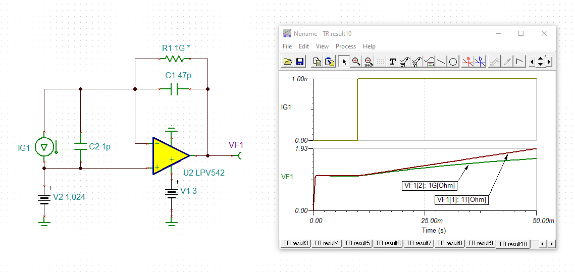
I'm using this op-amp to integrate a very small photocurrent.  The signal ramps up for about 40ms.  C3 holds the integrated signal until U3 (analog switch) resets the integral, and then the process repeats.  

Not shown:  The output directly drives an ADC with a S/H cap of 10pF.

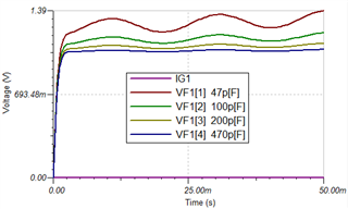
I've successfully used this method with the OPA336.  The new circuit uses the LPV542, which oscillated wildly.  I inserted R3 into the circuit to reduce these oscillations.  The placement of R3 as an isolation resistor isn't exactly as shown in the LPV542 datasheet figure 38.  While the figure shows R(iso) after the feedback, I put R3 inside the feedback so the output is isolated from the feedback capacitance.  (It was trial and error, and this seemed to work.)

However....

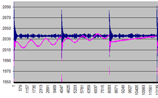
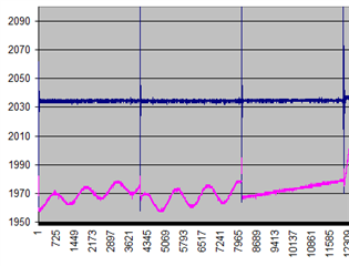
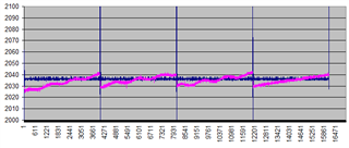
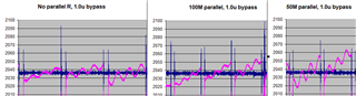
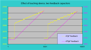
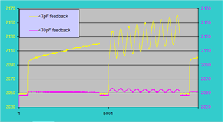
When the photocurrent is null, or close to zero, the circuit oscillates at 50Hz.  It's only a ripple (amplitude between 10-30mV) but annoyingly reproducible.  When there's even a slight photocurrent, it works as expected.  This isn't an antenna issue, as all the signal traces are tiny tiny tiny -- about the size of the component itself.

Did I do something wrong with R3?  And what more can I do to beat down the 50Hz oscillations?

Thanks so much for your expertise.

--zim

  • Hi David,

    R3 is at the wrong place. It should sit outside of the feedback loop. R3 shall isolate the output of OPAmp from capacitive loads being connected to signal ground. These would otherwise cause with the internal output impedance a phase lag in the feedback loop. C3 = 47p, on the other hand, is not causing an unwanted phase lag but a desired phase lead. Because of that you should not isolate the output of OPAmp from C3. C3 does good not bad Relaxed

    According to my phase stability analysis your circuit should run stably after removing R3.

    The reason for your 50Hz hum is that R3 heavily increases the output impedance of your circuit. Any EMI arriving at the output of your circuit cannot be short-circuited to signal ground any longer but causes a voltage drop across R3. That's why you have hum at the output. Decreasing R3 to 0R will heavily decrease the hum, I guess.

    Do you have any detector capacitance for the GUVB-S31GD? I assumed it to be much smaller than the stray capacitance of analog switch. Also, what is Vref and what is the supply voltage of OPAmp?

    Some tipps:

    It can be helpful to add some resistances to dampen ringing and to decrease charging and discharging current spikes. You could add a small resistor in series to the analog switch, 1k for instance. C3 doesn't need to be short-circuited but may profit from a non-zero discharging resistance. Also, mount a 1k resistor in series to the IN-pin of analog switch. Even a low pass filter to make the edges of switch signal less steep can be helpful. Remember, the LPV542 is a 8kHz nano-power OPAmp and doesn't like fast changes.  

    Kai

  • Hello Zim,

    I tried some simulation and it should be stable, although R3 is is the wrong place and probably not needed. Very low power op amps can be more difficult than other amplifiers. Can you try R3 from output to ground or op amp power?  Giving the output drivers a DC current and only using one of the drivers might help it behave better. If that works, but the supply current is too high, use a larger value resistor.

    Does "R3 reduces oscillation" mean it is still there?  Please provide the oscillation waveforms. 

  • Hi Kai,

    Thanks for your advice.  I suspected I had done something wrong with R3, but it's good to hear from someone who knows.  I'm hesitant to add more R's and C's, because I have very little board space, and I'm already using 0402s. I've tried something that (I think) follows what you suggested.

    I tried moving the right leg of C3 to the node between the op-amp output and R3.  This removes the increased phase lag, while still isolating the switch and the ADC from the op-amp.  It even adds series resistance to the discharge through the switch.  There is a small offset caused by the photocurrent passing through R3, but that doesn't bother me as it's only when the switch is closed, and it's less than 1 LSB.

    Didn't solve my problem though.  The first 2 panes show the circuit with no photocurrent, the last 2 have a tiny amount of light.

    Answers to your other questions:  The photodiode datasheet does not specify capacitance.  Vref is 1.024 volts, Vcc is 3 volts.  Both are bypassed to GND via 0.1uF caps.  (I know I should have bypassed Vcc to Vref instead.... would this make a significant difference?)

    Any other ideas I should try?

  • Hi Ron,

    Thanks for your response.  That was a good idea to load the output of the op-amp, but it hasn't changed the result.  I first tried a 1M resistor to ground, and then a 50k, but there's no change.  (These tests were done after implementing Kai's suggestion.  See above for details.)

    Here are the waveforms, before and after the loading.  The offset appeared after Kai's mod -- I don't know why.  500uV per count, 63.8 kHz sample rate:

    The last pane of each shows the effect of adding a minimal amount of light to the photodiode.  It's like magic.  

    "R3 reduces oscillation" means it still oscillates, but only when there's no photocurrent.  

  • Some progress....  This is the result with R3=0, and a 1M resistor from the output of the op-amp to ground:

    The amplitude has been reduced to about 4 LSB.  Oscillations are still there, except for the last frame where I allowed it to see some minimal light.

  • Hi David,

    very interesting.

    Without any light the photo diode becomes very high ohmic. And as you don't have any feedback resistance, the whole feedback path becomes an extremely high ohmic antenna. You could try to add a high ohmic resistance in parallel to the photodiode and/or in parallel to C3.

    You could also add some Faraday shielding: Enclose the whole circuit by a metal box (at least aluminium foil) and connect it to the ground pin of OPAmp. Open the shielding only at the optical window of photo diode.

    There could be another issue. You say your reference voltage is 1.024V? The reference voltage should supply the OPAmp circuit low ohmically. How do you provide that?

    Also, if the 1.024V is generated by a voltage reference chip then keep in mind that some voltage references don't like capacitive loads and can become instable. Others allow capacitive loads but only in a certain range.

    More, some don't like zero load current situations or become instable because of the capacitive loading only at certain load currents.

    So, it could be wise to put eye on the 1.024V generation. You could scope Vref. Do you see any hum there? You shouldn't...

    Kai

  • David,

    Kai has a great point. With no light or photo diode removed, the circuit becomes an input bias current self-measurement circuit. When I've made one of those, I had to stay 4 feet away or put it in a cage to prevent measurement corruption. It's just that sensitive. With even a little light current, the diode also becomes a current source. There is no such thing as a perfect current source, all will have some finite (parallel) impedance. This finite impedance will lower the total impedance at the inverting input. So it's not really magic. Slight smile

    Try no light and sync your scope to line frequency, I believe your will find that the 50Hz is air pickup, not an oscillation.

  • Hi Kai and Ron,

    Now *that* makes sense!  I just tested the last version of the circuit (R3=0, with 1M added from OUT to GND).  Here are the results:

    The first two panes are with overhead fluorescents turned ON, and the device in an aluminium box.  (The box is not a perfect shield, because the top and bottom halves are painted, and not in electrical contact with each other).  

    Pane #3 shows what happens when I open the box and touch the device.

    Pane #4 shows when I pick up the device with one hand (covering the sensor) while extending the other hand over my head as an antenna.

    Panes #5-8 repeat #1-4, but with the overhead lights turned OFF.  (I did put my hand in the air during #7, so that's why it looks the same as #8).

    Note that the blue trace is tracking Vref.  No problems there, but that was a good thought to check it.

    All this makes it pretty clear that Kai's analysis is correct, and the input is essentially floating.  (Duh, now that I think about it.)

    I would love to add an ohmic element somewhere to keep this from happening.  The problem with putting it at the input (in parallel with the photodiode) is that the photocurrent is ~1pA to ~1nA, so a resistor would need to be several G-ohms to T-ohms so it doesn't dominate.  The problem with putting it in the feedback loop (parallel with C3) is that it makes the math very messy, and totally changes the nice, clean ramp of the integral.

    Thinking about this second option, is an integrator with a parallel resistor still an integrator?  With an infinitely high value of R, it is.  As R falls, the system behaves more and more like a standard transimpedance amplifier, with C3 behaving more like a filter and less like an integrator.  I remember there is some complex math in the transfer function, making it hard to work out what the photocurrent is.  Some help here?

    Would a capacitor in parallel with the photodiode work?  Pass the air pickup to GND, without introducing any DC offset?

  • See my response to you and Ron, above.

  • Hi David,

    Thinking about this second option, is an integrator with a parallel resistor still an integrator?

    Most of all real world integrators I know have a resistor in parallel to the integration resistor in the feedback loop. The key is always to find a balance -or better said- compromise between the integration capacitance and parallel resistance. It's the time constant which counts, or the corner frequency, if you treat it in the frequency domain.

    Best you choose a proper integration capacitance and parallel resistance by trial and error. There are formulas indeed, but they never "know" in detail what is important for you Relaxed

    Maybe it's interesting to mention that the parallel resistance plays no role when the integration capacitance is uncharged. No voltage drop no current. The more the integration capacitance becomes charged, the more current flows unwantedly through the parallel resistor then.

    To minimize the error due to the parallel resistance the current through it should be way smaller than the current through the integration capacitance, of course. The current through the integration capacitance can be estimated by:

    Ic = C x dUc/dt

    And the current through the parallel resistance can be calculated by:

    Ir = Uc / R

    "dUc/dt" can be read out of your above plots. From this "Ic" can be estimated. And from the voltage "Uc" at the end of sampling interval "Ir" can be calculated which would flow with a chosen parallel resistance "R". This very simple method is correct enough to get a feeling of how big "R" should be chosen.

    Kai 

  • To minimize the error due to the parallel resistance the current through it should be way smaller than the current through the integration capacitance, of course.

    That's the problem.  The current through the integration capacitor is 1nA.  The integral takes about 50ms to reach 1V through 47pF.  (And this is when the signal is maximum!)

    Sorry, I can't afford to waste any of that signal by shunting it through a parallel feedback resistor.  Besides, 100G resistors aren't cheap.

  • Hi David,

    yes, because your integration cap is unusually small, even 1GOhm would still be too small:

    david_lpv542.TSC

    Eventually, a resistor in parallel to the photo diode can do the trick?

    Kai

  • David,

    Can you take your start and stop measurements in sync with the 50Hz, ideally at zero crossing? (may be 60Hz in other parts of the world). There may be other math solutions to remove 50 and 60 Hz. The easiest is to make measurement period 100mS; this would be in sync with both 50 and 60 Hz. 

  • Hi Kai,

    That's an elegant solution, putting the R in parallel with the photodiode.  I tried it, although I didn't have a 10M, so I used a 1.74M.  It shouldn't matter, as delta-V is zero between the inputs, so no current should flow if everything works according to physics.

    Results:  It didn't work.  The integration was smooth, but the results were not as expected.  In total darkness, the integral ramp was steeper than the ramp with some light applied. (Quite significantly!)  So I think we're playing with some marginal non-ideal characteristics of the op-amp and photodiode.

    Thinking more about it, I'm not sure the problem is with the INV input being "open".  Isn't the feedback cap keeping the INV input from drifting?  As the output bobs up and down at 50Hz, wouldn't that be passed to the INV input via the cap?  Also, I've now found the 50Hz ripple when there's photocurrent, but it's only visible if I charge myself up by rubbing my sleeves together.

    I'm looking into some issues with Vref.  It turns out I've taken Vref from an MCU pin that has some impedance.  Maybe that's causing the ripple. 

    Thanks again for your help. 

  • Hi Ron,

    Good idea, thanks!  I'll give it some thought, but it would be best to eliminate the pick-up altogether.

    The integration time (start-to-stop) is now around 40ms.  If I resize the feedback cap, 100ms might be okay. 

    However, the sensitivity of the photodiodes vary quite a lot within a production batch.  I've been normalizing the instruments' signal responses by adjusting their integration times in software.  A fixed integration time would cause huge variability in photosensitivity between instruments.  (I could choose each integration cap to normalize the photosensitivity, but that's messy and would create a problem for manufacturability-at-scale.)

    Still trying to eliminate the ripple.

    [edit]  Thinking while walking the dogs, I realized that I could measure at 100ms, and then scale the result in software.  Resolution and SNR would suffer, because I would need to size the integrating capacitor to keep the fastest photodiode within the rails. Slower photodiodes would only utilize maybe 20% of the available dynamic range.  Not ideal, but few things in life are.

    [edit edit]  After walking the dogs some more, I realized that for the less sensitive diodes -- at least the ones that result in measurements less than 1/2 of the range of the ADC -- I could integrate for another 100ms cycle.  This would increase resolution of the bottom half of the scale, essentially giving me another bit.

  • Hi David,

    no, 1.74M is too small. Keep in mind that the impedance of 47pF cap at 50Hz is 68M. So the resistance in parallel to the photo diode should be in the same range, otherwise you create a gain for the hum. I think 10M is the minimum you should use.

    Here the result of simulation with 1.74M:

    And here with 100M:

    Kai

  • Thanks Kai, I'll try it.  It might be a week or two to source some high-value 0402's.  I'll let you know when I do.

  • Hi David,

    I would take a 10M or 22M thin film resistor.

    For a quick test you could put some of your 1.74M in series Relaxed You should already see a difference with two or three of them.

    Good luck.

    Kai

  • Kai, I tried a 100M 0805 resistor.  The resistor does not appear to do anything.  The 50 Hz hum is still there.  I'll try two R's in parallel to make 50M, but I am starting to lose faith.

    I've been playing with your TINA file, to better understand why 1.74M behaves as it does.  I ran the TR analysis for the 1.74M and 100M, and the 1.74M shows a rising output before the input rises.   I don't see why this would happen. 

    Also, questions for how to use TINA:

    1.  I accidentally changed something so the input steps from 1nA to 2nA -- I can't find where to change this back.  IG1 is set to 0 DC, unit step of 1nA. 

    2.  The analysis graphs a range of input conditions, so the output is fanning out.  I can't find where to turn this off.

    Thanks again for your advice.  You've been terrific.

    1401.david_lpv542.TSC

  • Results for the 50M resistor:  No change.  

    These test conditions are not identical, so the amplitude changes a bit.  But the 50 Hz hum is still there.

    1.024v / 50M = 20nA.  This is 20x more current than the photodiode draws.  I think the source of the hum is somewhere else.

    [edit]: The graphs say "1.0uF bypass".  This is on Vref.

  • Hi David,

    1.  I accidentally changed something so the input steps from 1nA to 2nA -- I can't find where to change this back.  IG1 is set to 0 DC, unit step of 1nA. 

    You have unwantedly modified "IG1" with the "select control object" command. "IG1" is marked now by a small cross. Best "delete" it and copy and paste "IG1" from my TSC-file.

    Kai

  • New question:  I have rearranged the circuit, and added a 1k and 100nF at the output:

    This has improved the performance of the ADC, but also added a 10mV oscillation at around 2.7kHz.  Any suggestions for how to nip this?

    I'm still working on the 50Hz hum, but the output impedance was a bigger problem to solve.

  • Hi David,

    can the 2.7kHz oscillation only be seen when the ADC is connected and running?

    Referring to the 50Hz hum: I would extend the Faraday cage over the whole circuit, including the microcontroller. Even additional local shielding between the OPAmp circuit and the microcontroller can help. Check the shielding: When the whole circuit is shielded (even without any opening for the photo diode !) the 50Hz hum should disappear. And, important: Avoid loops creating multiple connections between the shields and signal ground. This would create loops where magnetic fields can again induce currents. You can add local shieldings inside the Faraday cage, but avoid them from creating any closed loops.

    You could also use a solid ground plane for your circuit. But separate the analog circuitry from the digital circuitry.

    Can you post your layout and a photo of your setup?

    Kai

  • Hi Kai,

    Sorry for the delay.  I hesitate to use a Faraday cage to solve this, because of cost and manufacturability.  The circuit is so small, and the board area inside the feedback loop is incredibly minimal.  I don't believe it's a layout or ground-loop problem, but I'll look there next.

    Thanks to your post above, I've been attacking the problem with TINA-TI.  First, I added the photodiode's non-ideal passive elements, but I had to guess at the values.  (Luckily, when I change these values, it doesn't affect the output very much, so I don't think these are critical.)  

    Next, I modeled the modified circuit I described in my last post.  (Reminder: when tested in hardware, this circuit works well except for some HF noise around 2.7kHz.)  I've found this:


    In the model, there's a large increase in gain where the phase crosses 180 degrees, right around 3.7kHz.  This isn't quite 2.7kHz, but pretty close.  In the model, increasing the value of the series output R2 to 5k makes this go away, and the Bode becomes flat like it should be.  I'm testing this in hardware today, to see if it makes the HF oscillation disappear.

    Also using TINA-TI, I've found something that might help with the 50Hz hum.  I added a 50Hz signal to IG1, and changed the feedback cap to look at the effect on the output:

    When the value of the feedback capacitor increases, the hum is greatly reduced.  This is true in hardware as well. 

    Thanks for reminding me about TINA-TI.  It's much easier to try different solutions when each modification is virtual instead of soldered into hardware. (Virtual = seconds per iteration, versus hours for hardware tests.)  Now that I have an idea what to modify, I'll try it in hardware.  I'll let you know how it goes.

    --zim

    david3_lpv542.TSC

  • Really good work, David Relaxed

    I have estimated the detector capacitance of GUVB-S31GP to 1pF because of its extremely small sensitive area of only 0.076mm^2. Compared to the BPW34 with its sensitive area of 7.5mm^2 this is about 100 times smaller and would give an about 100 times smaller detector capacitance than the 70pF of BPW34 resulting in about 0.7pF.

    Such a small detector capacitance would explain why it is not specified in the datasheet. It would be in the range of normal layout stray capacitance and would even exceed the input capacitances of the most OPAmps.

    But as being an UV-light photo diode the effective thickness of depletion area within the photo diode could be way different compared to a standard photo diode. So I think it would be a good idea to ask the manufacturer for the detector capacitance.

    Kai

  • The hardware trials are complete, and they confirm the TINA model.  Here is a graph of two very small signals being integrated.  The pink line integrates ~1nA, the yellow line integrates ~3pA.  (Yes, pico-amps!!!) 


    The integration time is roughly 170ms, which is approximately 8.5 cycles of 50Hz.  You can see the 50Hz pickup in the second integration cycle, when I touched the device with my hand.  

    The above comparison between the two feedback capacitors isn't quite fair, because the same 50Hz pickup that grossly affects the 3pA photocurrent (yellow) is totally swamped by the 1nA photocurrent (pink).  The two lines are graphed on different scales, which further obscures the results.

    When the same test is performed in the dark, the result shows a more fair comparison:

    I had to "charge myself up" by rubbing my sleeves together to make the 50Hz pickup large enough to see.  But since the two photocurrents are both zero, the result is only affected by 50Hz pickup and some non-ideal behaviour in the op-amp.  This makes the two channels directly comparable on the same scale.  This shows that the value of the feedback capacitor affects the amplitude of the 50Hz pickup.  

    This data was obtained using an on-board 12-bit ADC.  The ADC includes an internal 10pF S/H cap that is shown at the far right of the circuit schematic.  There are no external leads or wires to any analogue signals.  The board layout optimizes analogue trace lengths, which are all 15mm or less -- much less in the case of the op-amp inputs. 

    Perhaps we can do more to prevent the 50Hz pickup by using shield traces and ground planes.  That comes next.  The help we received in this forum has been brilliant to help us understand what we're seeing.  Thank you to everyone who contributed.

    I think this post closes this thread, as the op-amp behaviour is now pretty well understood.  Cheers!

  • Well done, David Relaxed

    I only want to encourage you to use Faraday cage shielding. Shielding is our strongest weapon against EMI.

    Good luck!!

    Kai