This thread has been locked.

If you have a related question, please click the "Ask a related question" button in the top right corner. The newly created question will be automatically linked to this question.

INA338: SPICE model required

Part Number: INA338
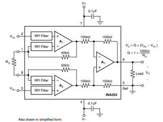
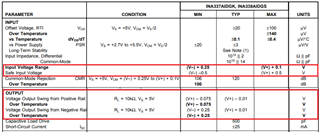
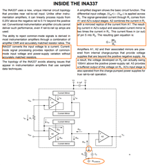
Other Parts Discussed in Thread: INA326, ADS131M06, INA333, INA337

Hello,

I have some uncertainty regarding INA338 instrumentation amplifier. Is there some verified SPICE model? I would like to simulate my circuit, to find confidence in it before ordering PCBs.

Thanks in advance,

Stanislav

  •  Hi Stanislav,

    Is there some verified SPICE model?

    Unfortunately, we do not have TINA INA337/INA338 PSpice model; however, we do have one for the INA326, which is similar to INA338, Please see the link below. 

    https://e2e.ti.com/support/amplifiers-group/amplifiers/f/amplifiers-forum/918676/ina337-ina337-output-information?tisearch=e2e-sitesearch&keymatch=ina337#

    Below is the INA338's Vcm vs. Vout plot to create a linear response from output to input. You may download the tool in the link below.   

    https://www.ti.com/tool/ANALOG-ENGINEER-CALC

    If you have any additional questions, please let us know. 

    Best,

    Raymond

  • Hello Raymond,

    Thanks for your reply. While this tool may be helpful, I am afraid it is not all I need. Theoretically, maybe I will learn the rest from simulations of INA326 - but this part differs in output swing range near supply rails.

    I will explain what I need. Supply voltage 5V. At input side, I want to interface with load cell, which has Vcm of 2.5V and Vdiff of +-5mV full-scale.

    At output side, I want to interface with ADS131M06 (supplied with 3.3V). I intend to connect IA's reference and ADC's inverting input to ADC's reference. Then IA's output to ADC non-inverting input. Here I need to know allowed output range of IA when powered by 5V single supply, referenced to positive voltage.

    I also have confusion with how to correctly connect reference voltage to IA. I will explain it on INA338's datasheet.  At figure 1 on page 9, pin 5 is connected "directly" to reference voltage using parallel RC element in series. At least this is how I understand it. I suspect this does not need to be ground, because this connection is independent of single/dual supply operation.

    However, following is figure 6 on page 12, mentioning output range pedestal using voltage divider. Here I totally do not understand where is the difference, and what is required in my scenario.

    Stanislav

  • Hi Stanislav,

    Here is the design requirements.

    1. Single power supply rail: 5Vdc

    2. INA338's output voltege: 3.3V_max. 

    3. Vdiff_max = 5mV and Vcm = 2.5Vdc. 

    Estimation about the Gain: 3.3V_max/5mV = 660 V/V_max.  

    If your 0<= Vdiff <= 5mV, then you will require a small Vref voltage, say 0.1 to 0.25Vdc. If your 200uV< Vdiff <= 5mV, then you may leave Vref = 0 Vdc. 

    The two scenarios are demonstrated in the Analog Engineer's calculator.  By increasing by Vref, you may alter the input and output ranges for your application. These are simple comparisons.  

    I will simulate a condition with Gain = ~600V/V and Vref = 0.25Vdc using INA326.

    The final Gain per simulation is 570V/V and I did not fine tune it further. You can adjust it and make what you'd like. 

    BTW, the circuit may require additional LPF filter at INA338's output for interfacing with ADS131M06 properly. Please ask ADC support team for the additional support. 

    INA326 5Vdc for INA328 06162022.TSC

    If you have additional questions, please let me know. 

    Best,

    Raymond


  • Hello Raymond,

    Now I understand how I can use the tool. Only one thing, does it detect all violations for IA's parameters? More specifically I am interested at behaviour near 0V output.

    However, I am still confused when it comes to applying reference voltage to IA. Could you explain the difference between figures mentioned in my previous post?

    Stanislav

  • Hi Stanislav,

    does it detect all violations for IA's parameters?

    Yes, the Vcm vs. Vout tool is taken into account all the linear operating parameters found in INA338's datasheet. You may go through the INA338's datasheet and you will find that the tool is making a design much easier. 

    More specifically I am interested at behaviour near 0V output.

    If you want to have Vout = 0Vdc with  Vin = 0Vdc, then you may have to use a negative supply rail as shown in the datasheet. You may use LM7705, a switched capacitor voltage inverter to apply -0.232V or lower on the V- supply rail. Based on the datasheet requirements, the Vout is V- + 0.25V over the entire temperature range. I would recommend to apply -0.4Vdc to -0.5Vdc at V-, so that Vout has a design margin to go down to ground or Vout = 0Vdc when Vin = 0Vdc.  

    Alternatively, you may use what I have simulated with an elevated Vref when Vdiff_input = 0mV. 

    However, I am still confused when it comes to applying reference voltage to IA. Could you explain the difference between figures mentioned in my previous post?

    The IA's transfer function is Vout = Gain*(Vin+ - Vin-) + Vref. In the simulation example, (Vin+ - Vin-) = 0mV and Vout = 0.25V when Vref is configured at 0.25Vdc for a single supply rail. For dual or asymmetrical supply voltage rails, Vout =  Gain*(Vin+ - Vin-) with Vref = GND = 0Vdc. 

    The application note below describes how two op amp IA is designed and operated. You may play around the attached simulation to have a better understanding how it works.

    OPA192 2-op amp IA 06162022.TSC

    https://www.ti.com/lit/an/sboa281/sboa281.pdf?ts=1655417707671&ref_url=https%253A%252F%252Fwww.google.com%252F

    If you have additional questions, please let me know. 

    Best,

    Raymond

  • Hello Raymond,

    Unfortunately, you still did not answer my question. Now I believe I know the answer.

    What I was asking, I can see that you are applying voltage to pin 5 using a voltage divider. Is this just about generating lower voltage from higher?

    In simulation, I have applied my reference voltage using only single resistor (and its filtering capacitor), and it is working just fine, even without voltage divider. This is preferred setup for me, I do need reference voltage source for more reasons(including ADC reference).

    Stanislav

  • Hi Stanislav,

    INA338 is a 2-op amp instrumentation amplifier, see the Gain equation below in blue. In 2-op amp IA circuit, Gain = 2(R2/R1). Without R2 resistor, no gains may be configured. This is how gains are Vref are implemented when configuring in 2-op amp IA circuit. 

    Below is 3-op amp IA circuit. I think that what you mentioned is 3-op amp IA, not 2-op amp IA type. In 3-op amp IA, yes, the Vref (a low impedance node) may directly apply to pin5 as shown in INA333's datasheet. 

    Is this just about generating lower voltage from higher?

    Not really, though this is a side effect since the IA's transfer function is Vout = Gain*(Vin+ - Vin-) + Vref. With higher Vref, Vout will also increase. 

    Have you altered Vref in INA338's Vcm vs. Vout graph in a single supply rail configuration? Please pay attention to the parameters that marked in the prior reply. Any Vcm vs. Vout conditions within the boundary of the diagram is considered linear operation, which is the same as the performance figures presented in the INA338's datasheet, see the captured image below. Please pay attention to Vdiff_min, Vdiff_max, Vout_min and Vout_max ranges as Vref is changed, when other IA settings are fixed. 

    Best,

    Raymond

  • Hello Raymond,

    We still do not understand each other. I understand that R2 is mandatory to achieve gain. I also understand effects of Vref on Vout.

    Here is my schematic, which I would like to confirm. Please observe that I do not use R2' resistor. One end of R2 resistor is connected to IA:7 (INA338 in MSOP-10 is used), the other to reference voltage (coming from reference voltage source on another board).

    In contrast, some figures in datasheet, and your schematic, uses additional resistor R2', which applies reference voltage to IA:5(respectively 7 on INA338), R2 is connected against ground. Is R2' mandatory, or is it just a trick to generate lower Vref voltage from some higher voltage (maybe supply voltage)?

    Stanislav

  • Hi Stanislav,

    Is R2' mandatory, or is it just a trick to generate lower Vref voltage from some higher voltage (maybe supply voltage)?

    Ok, I see what your question is. You should have posted the schematic from the get-go. 

    Pin5 is a node can swing +100mV above V+ rail and -20mV below GND or negative supply rail as described in the INA338's datasheet. In other words, the voltage developed on R2 or pin5 has to have ability to source or sink in current (2I_R1 is up to -20mV/R2 for sourcing and +100mV/R2 for sinking in current). In addition, ground connection is the current common mode reference for the INA338.   

    The internal circuit of INA338 (same as INA326), the feedback is in current not in voltage as presented in the section of "INSIDE THE INA337". If you inject a low impedance Vref at pin5 node, the circuit probably will still work, see the orange circuit (equivalent to voltage divider). 

    If the Vref signal is injected from the opposite end of R2 (as pictured in schematic), then the operation may generate errors. It probably will still operate, but it may create unknown errors (2I_R1 and IAcommon errors).

    If you have other questions, please let me know. 

    Best,

    Raymond

  • Hi Stanislav,

    Is R2' mandatory, or is it just a trick to generate lower Vref voltage from some higher voltage (maybe supply voltage)?

    It's just a trick to generate a small pedestal (pseudo ground) from a bigger reference voltage.

    Kai

  • Hello Kai,

    Thanks for your reply. This is what I wanted to confirm.

    Stanislav