This thread has been locked.

If you have a related question, please click the "Ask a related question" button in the top right corner. The newly created question will be automatically linked to this question.

THS4567: Application Help

Part Number: THS4567
Other Parts Discussed in Thread: TINA-TI

Hello Team,

I'm posting on behalf of my customer, please see the inquiry below:

Hello,

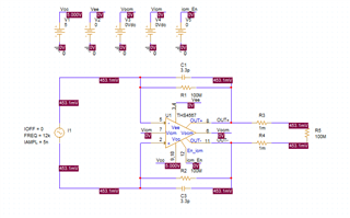
I built the circuit in the figure on a four-layer PCB, replacing R1 with an AD8338 variable gain amplifier.

I used a single 5V supply and connected ICM EN to gnd.
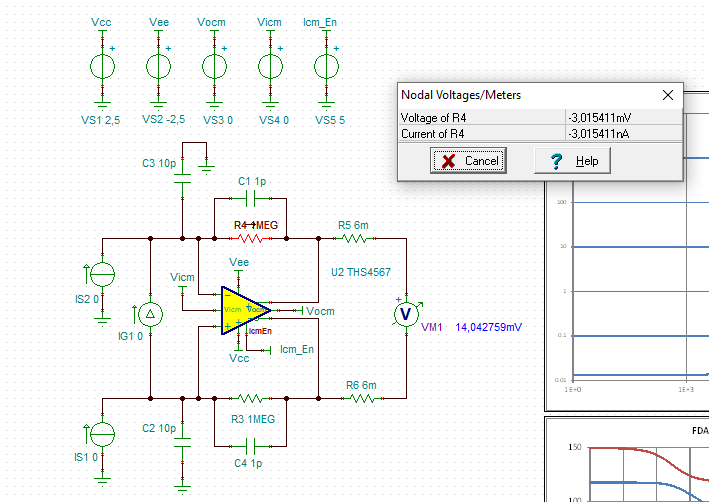
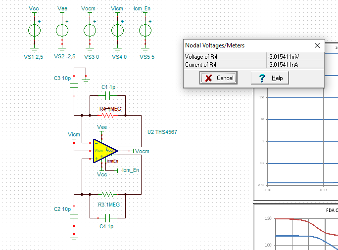
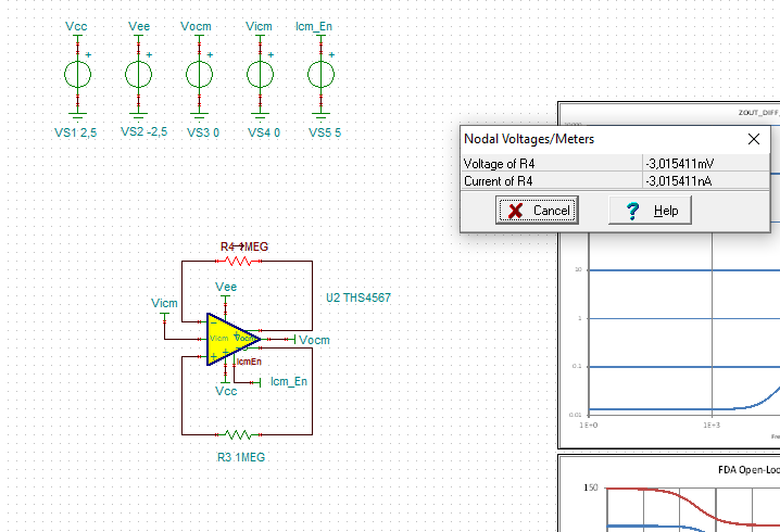
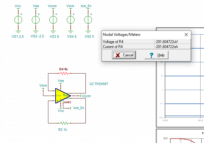
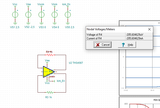
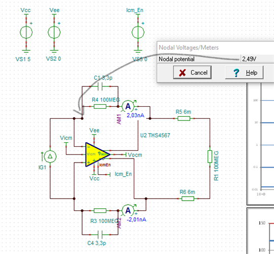
I'm investigating why I'm getting 20nA on the feedback path.

Actually, I'm getting 0.5V on the inputs and 2.48V on the outputs.
On the datasheet, I see a much lower current than what I get (in the order of pA).

Regards

Renan

  • Hello Renan,

    I will take a look and get back to you with any questions.  Could you confirm the model version/year for the THS4567 SPICE model?

    Best,

    Alec

  • Hi Alec,

    the TINA-TI reference design is also showing issues.

    Kai

  • Hi Kai,

    Thank you for confirming this; I will investigate and update you.

    Hello Renan,

    I will come up with some questions and ideas for you shortly.

    Best,

    Alec

  • Hello Renan,

    I have several follow-up questions in order to clarify what is happening here:

    1. Are you referencing measurements in simulation or on a fabricated PCB?  Could you clarify which measurements correspond to which?

    2. What is your VOCM pin voltage, and your VICM pin voltage?

    3. What are your measurements at the inputs/outputs?

    4. What are your intended signals at the inputs/outputs?

    5. What is the setup for the current source present in your circuit?  Does it have a DC component, or just AC?

    6. Is your design referencing the Differential TIA with 0-V Biased Photodiode setup in figure 8.7 for your design?

    7. Could you share a complete circuit simulation file?

    For concerns with your PCB, could you share a schematic or board file?  If not, could you confirm what you are measuring on the PCB?

    I know this is a lot of questions, but these will help me zero-in on where you need help.

    Best,

    Alec

  • Hello Alec,

    Please see my customer response below:

    1. Are you referencing measurements in simulation or on a fabricated PCB? Could you clarify which measurements correspond to which?

    I'm referencing measurements on fabricated 4-layers PCB.
    On the PCB ICM_EN is at GND. I'm measuring voltages on PIN 4 (IN+) and PIN 6 (IN-) and I'm getting 0.5V. On Spice model I'm getting 2.49V. Moreover on PCB I'm getting 2.48V on PIN 1 (OUT-) and PIN 9 (OUT+) while in spice I'm getting 2.69V. My feedback resistor is a 100e6 ohm resistor so I'm getting 20 nA on the feedback path.

    2. What is your VOCM pin voltage, and your VICM pin voltage?

    VOCM = 2.48V
    VICM = 1.5V

    3. What are your measurements at the inputs/outputs?
    4. What are your intended signals at the inputs/outputs?

    I'm trying to built a standard CSA fully differential preamplifier for Quartz Tuning Fork (QTF) that generate a sinusoidal current (we don't know exactly it's characteristics) in response to an external excitation so I disabled the input

    5. What is the setup for the current source present in your circuit? Does it have a DC component, or just AC?

    As I said, my current source is a Quartz Tuning Fork that is a piezoelectric sensor, so the mechanical strain generates a certain amount of charge at its terminal. It can be modeled by the Butterworth-Van Dycke model for piezoelectric crystals (RLC with an AC source and a parasitic capacitance in parallel).

    6. Is your design referencing the Differential TIA with 0-V Biased Photodiode setup in figure 8.7 for your design?

    More or less, yes.

    7. Could you share a complete circuit simulation file?
    Yes, of course, I'm sharing also the pcb schematic file.

    ADM_Preamp_V2_Schematic.zip

    Regards,

    Renan

  • Hello Renan,

    Thank you for this information Slight smile.  I will take time to look this over and generate a response; I'll ask follow-up questions if I have any.

    Best,

    Alec

  • Hi Alec,

    here are some results I get with the

    THS4567 TINA-TI Reference Design Circuit

    if that helps:

    Kai

  • Hello Alec,

    Good day. Any update you can give us regarding this issue?

    Regards,

    Renan

  • Hello Renan,

    I am looking into this behavior tomorrow.

    Best,

    Alec

  • Hello Alec,

    Any update?

    Regards,

    Renan

  • Hello Renan,

    I am checking with my team on some items regarding your signal source (quartz tuning fork).  I am also looking into some of the model behavior Kai displayed in the TINA-TI images.

    Best,

    Alec

  • Hello Alec,

    Any update on this?

    Regards,

    Renan

  • Hello Renan,

    I believe I am getting more sensible values in relation to your PCB measurements in PSPICE for TI; this could be a model difference or simulator artifact.  The higher 100 MOhm feeback resistors could be magnifying the bias current and resulting in a higher Ibias/current at feedback node.  

    Could you clarify whether your customer's measured PCB values are incorrect/unacceptable vs. not matching simulation?  What would your ideal performance values be for your implementation?  For example, when ICM loop is disabled, there should not be a voltage on that pin.  My PSPICE simulation reflects this behavior.  

    I can help adjust your simulation or design to match what performance characteristics you need.

    If my screenshots/attached file does not capture the simulation parameters correctly, please correct or inform me of such so I can best replicated your intentions.

    Please see the following screen-caps from PSPICE for TI:

    Voltages:

    Currents:

    SPICE Files:

    pspice_ths4567.zip

    Best,

    Alec

  • Hello Alec,

    Please see my customer update below:

    At the input, my measured PCB values are incorrect. ICM EN = 0V should give me 1.5V at the input feedback, but I only get 450mV. That's what the voltage picture show, but I also have 1.5V on VICM. This pin is set to 0V in your simulation.
    ICM_EN is 0V on my PCB.

    Regards,

    Renan

  • Hello Renan,

    Thank you for the customer update.  I will investigate with the ICM EN & VICM values in their setup.

    Best,

    Alec

  • Hello Renan,

    Please see the attached PDFs which have been updated to use VOCM = 2.48V and VICM = 1.5V; with ICM_EN = 0V.  I think we are establishing a bit more parity with our simulations; however I must ask a clarifying question or two:

    1. Could you confirm the values/parameters for the AC current source you are using for simulation?  Is there a DC offset or set value (AC or DC) for simulation purposes? I want to make sure I am injecting the correct input signal into the model.

    2. I see that you are measuring 0.5V on the PCB at the IN- and IN+ pins of the amplifier, which show up as 2.5V in my simulation.  Since the input common mode is disabled for your use case, these nodes are affected by the voltage seen across the feedback network from the output.  When you measure the PCB, is the remaining portion of the signal chain also powered?  Our simulation tactics may not be accurate to how the other pieces of the circuit are behaving on the PCB.  

    schematic_current_bias.pdf

    schematic_power_bias.pdf

    schematic_voltage_bias.pdf

    Best,

    Alec

  • Hello Alec,

    Please see my customer response below:

    "Could you confirm the values/parameters for the AC current source you are using for simulation? Is there a DC offset or set value (AC or DC) for simulation purposes? I want to make sure I am injecting the correct input signal into the model."

    Yes, I can confirm the values and the parameters for the AC current source. No, there isn't any DC offset.
    You could inject also 25nA input signal into model.

    "I see that you are measuring 0.5V on the PCB at the IN- and IN+ pins of the amplifier, which show up as 2.5V in my simulation. Since the input common mode is disabled for your use case, these nodes are affected by the voltage seen across the feedback network from the output. When you measure the PCB, is the remaining portion of the signal chain also powered? Our simulation tactics may not be accurate to how the other pieces of the circuit are behaving on the PCB."

    Yes, the remaining portion of the signal chain is also powered but the output pins show the right voltage (2.48V). Also all the other voltages around the chain are correct.

    Thank you and have a good day

    Regards,

    Renan

  • Hello Renan,

    Thank you for checking with your customer; I have a couple ideas about what to troubleshoot and verify now based on our discussion.  With your customer's design, what are the key items related to performance which your customer is concerned about?

    For example, they may have a strict power budget.  What needs to change about the current hardware to get the customer's design back on track?

    If I know what your customer is looking for out of their hardware implementation, we may be able to help them get the performance they want in parallel to figuring out the simulation portion of this issue.

    Best,

    Alec

  • Hello Alec,

    Good day please see our customer response below:

    "With your customer's design, what are the key items related to performance which your customer is concerned about?

    For example, they may have a strict power budget. What needs to change about the current hardware to get the customer's design back on track?"

    We don't have a strict power budget, but the board must be powered by 5V.
    We don't have any issues with 0.5V on the IN+ and IN- pins, but we'd like to know if there's anything we can do to fix this minor issue.

    Regards,

    Renan

  • Hello Renan,

    Thank you for checking with your customer.  I apologize for the lateness of my response;  I have been travelling and handling an influx of assignments upon my return.  As I see it, since the issue is not affecting the end requirements for the design, I can put a note to evaluate this model and its parameters if we end up revising it on our model roadmap.  This would not be a near-future item, but I will keep you posted if you wish.

    Best,

    Alec