This thread has been locked.

If you have a related question, please click the "Ask a related question" button in the top right corner. The newly created question will be automatically linked to this question.

INA823: Rail output for single supply 5V

Part Number: INA823
Other Parts Discussed in Thread: INA849

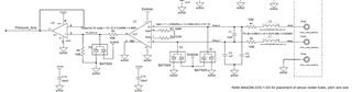
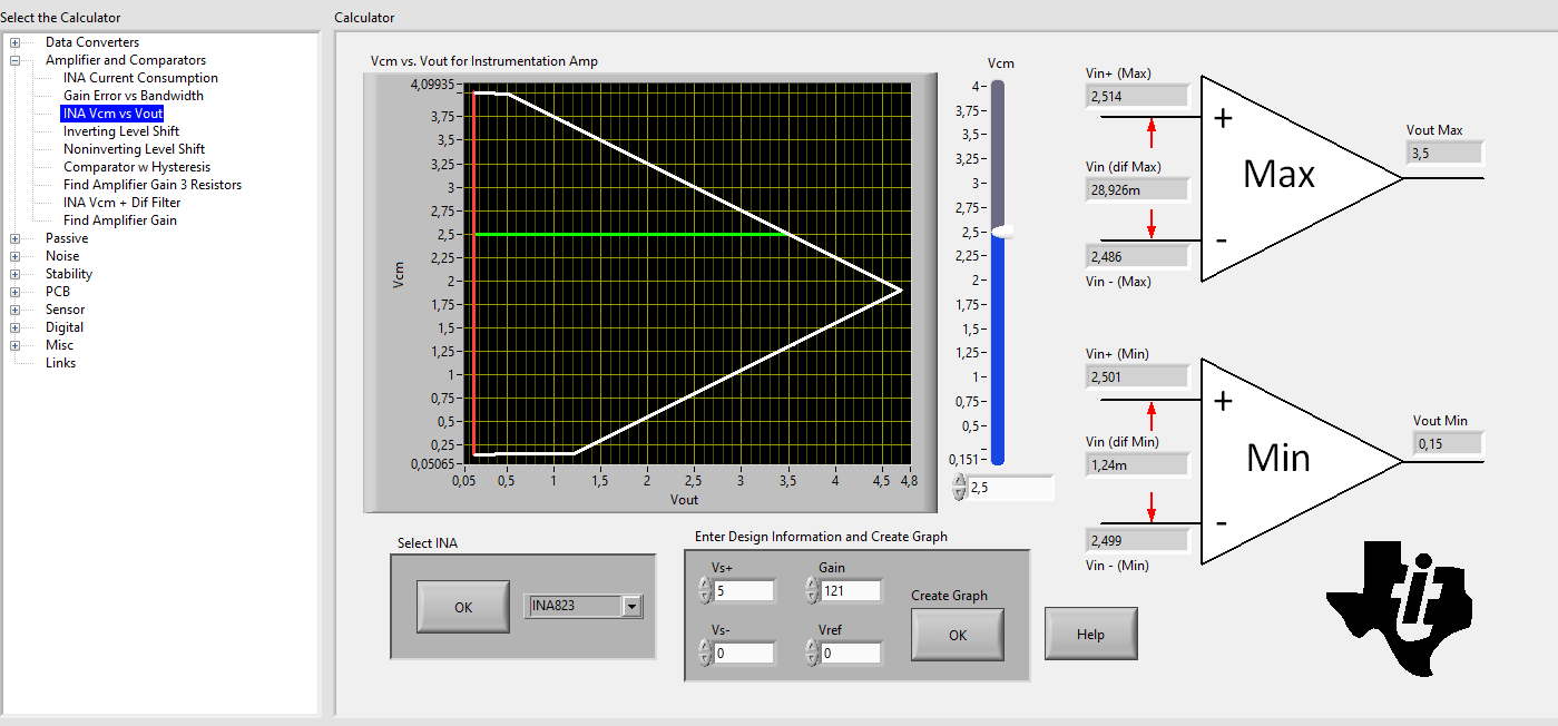
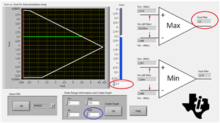
I got following output from INA823DR for different input. Attached circuit in the attachment.

10mV in = 1.2V
20mV in = 2.4V
30mV in = 3.6V
40mV in = 3.8V

The expected output for 40mV in is 4.8V.

Looks like INA823DR is hitting the rail output. 

From datasheet, output voltage swing +Vs - 0.15V = 5- 0.15 = 4.85V.

But it is hitting the rails at 3.8V around.

Pleas let me know your opinion. Thanks.

  • Hi Vintoh,

    the INA823 is no single OPAmp but contains three OPAmps. And these OPAmps can individually go into saturation while

    you will not be able to notice this from outside. Because of this TI has developed this "Vcm versurs Vout" calculator:

    See also this thread:

    https://e2e.ti.com/support/amplifiers-group/amplifiers/f/amplifiers-forum/1103241/ina129-ep-if-i-use-single-power-can-i-connect-ref-to-ground

    Kai

  • Hi Vinoth,

    Please following the link suggested by Kai. 

    You may reduce the input Vcm voltage to approx. 2Vdc or increase the Vref from the image below. When using the Analog Engineer's calculator, it will indicate the Vmin and Vmax output voltage for a given setting as marked in the graph below (as well as Vdiff_min, Vdiff_max input voltage range).  In your case, the max. of input differential voltage is configured at approx. ~29mV, but the actual Vdiff input of the setup is up to 40mV. 

    https://www.ti.com/tool/ANALOG-ENGINEER-CALC

    If you have additional questions, please let us know. 

    Best,

    Raymond

  • Hi Kai and Raymond, Thanks for your quick response.

    I bought few chips of INA823 and evaluated in bench.

    I am interested on the common mode voltage.

    Test condition: Gain : 121, Vs+ = 5V, Vs- = GND, Ref: GND.

    Input: No input applied across IN+ and IN-

    Measured Input IN+/IN- TO GND = approx 437mV.

    Shall I consider 437mV as input common model voltage?

    How to measure input common mode voltage (2.5V in previous chat)?

  • Hi Vinoth,

    I guess the 437mV is the voltage drop of input bias current of INA849 across the input resistance of voltmeter?

    Applying no input signal to the inputs of INA849 is no good idea. See section 9.1.1 of datasheet. No, if you want to measure the behaviour of INA849 at different common mode input voltages, then apply a common mode input voltage to both inputs by the help of a low ohmic source.

    Also keep in mind that in a single supply application connecting the REF pin to signal ground is NO good idea. In most cases you have to connect a pseudo ground potential low ohmically (!) to the REF pin to prevent the output going into saturation when applying a zero differential input signal.

    Kai

  • Hi Vinoth,

    Your initial INA823 configuration is very close. Your INA823's configuration should look similar to the schematic below. 

    What is your design requirements in INA823?" With 5Vdc in a single supply voltage rail, the output and INA823's gains are limited.  If your input differential voltage is up to 40mV, I would suggest to decrease the gain somewhat, say 100 V/V and configure Vref = 0.25V or so. Please follow Kai's suggestion and recommendation. 

    For a single supply rail setup, the current INA823 pspice model has a bug, so I am unable to show you the linear behavior via a simulation, but the recommendation from the analog engineer's calculator is correct and you should be able to follow the recommended parameters and repeat the INA823's performance on a test bench. 

    If you have additional questions, please let us know. 

    Best,

    Raymond 

  • Hi Vinoth,

    I am going to close this inquiry. 

    If you have additional questions, please let us know. 

    Best,

    Raymond