Because of the holidays, TI E2E™ design support forum responses will be delayed from Dec. 25 through Jan. 2. Thank you for your patience.

This thread has been locked.

If you have a related question, please click the "Ask a related question" button in the top right corner. The newly created question will be automatically linked to this question.

INA333: Application Inquiry

Part Number: INA333
Other Parts Discussed in Thread: ADS1220, OPA333, LM7705, REF3125, REF5025, REF5030, REF6025, REF34-Q1, MSP430F5529, REF3112, OPA387, LPV821, REF6250, TLV333, TLV2333, OPA4387

Hello Team,

My customer would like to know how the device will perform on their application below

(1) I am connecting ina333 referennce to midsupply of the whole circuit voltage using voltage divider( datasheet suggest me use low impedance soruce (15ohm) for reference pin) so I only have 10 ohm resistor avialable sso should it be fine without degrading the performance of ina333?
(2) if i connect the ina333 reference to midsupply, is there any way to level shif the code of ADC so that the zero value of adc is same as midsupply of ina333?
(3) I only have single ended positive voltage avialoable to power up the circuit and so my another concern is that if the reference voltage drift in ina333 then is there any way to compensate it the drift in ads1220 to get correct result?:

Regards,

Renan

  • Hi Renan,

    a schematic would be helpful.

    Kai

  • Hi Renan,

    (1) I am connecting ina333 referennce to midsupply of the whole circuit voltage using voltage divider...

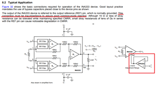
    Yes, if you use <15Ω voltage dividers at the reference pin will work, you may draw more current through the resistor dividers than necessary (INA333 is a low power IA). It is recommended to use OPA333 or other zero drift op amp to buffer a Vref voltage as a low impedance source (with source or sink capability at the output of the op amp). 

    (2) if i connect the ina333 reference to midsupply, is there any way to level shif the code of ADC so that the zero value of adc is same as midsupply of ina333?

    If you implement Vref at INA333's reference pin, you may have to level shift the INA333's output back to 0 to X Vdc range per ADC's input requirements. 

    Alternatively, you may use 3.3V or 5Vdc supply voltage to generate negative supply rail of -0.232V using LM7705 charge pump, see the attached application note. Since I do not have your design requirements, I am unable to simulate one for you. 

    https://www.ti.com/lit/an/sbaa373/sbaa373.pdf?ts=1657303709221&ref_url=https%253A%252F%252Fwww.google.com%252F

    3) I only have single ended positive voltage avialoable to power up the circuit and so my another concern is that if the reference voltage drift in ina333 then is there any way to compensate it the drift in ads1220 to get correct result?:

    Both INA333 and OPA333 are considered zero-drift op amps. In other words, the INA333's low drift performance is rated at 0.1uV/C with Gain >=100 V/V.  

    Please let us know the type of application that you are working with. If you want to have lower drift than the specification above, you may consider ratiometric ADC design approach. The attached application note is an example FYI. 

     https://static5.arrow.com/pdfs/2013/11/24/3/19/23/744/txn_/manual/slau520.pdf

    As Kai pointed out, it will be good to provide us with a schematic and the application requirements. 

    Best,

    Raymond

  •  Hello Raymond and Kai,

    Please see my customer response below:

    Ok I missed that detail of seeing opa333 as reference(i have no experince with op amps so I need to know something) if my supply voltage is 3,3 how do I set the opa333 to ouput midsupply for referenence?

    Now the level shifting of output of INA333 when using midsupply is not a problem assuming I have solved how to midsupply reference of ina333: here is what I did: I used one of the channel of ADS1220 and connected it to reference pin of INA333 when using Vref of INA333 and thus the adc output of that channel is subtracted from other channel output who is using ina333 output as input. Please tell me if this is also a way to do it? or am I doing a mistake by doing such thing. and also this all takes care of any drift or change in reference voltage problem?

    I have added schematic of what I have on my breadboard right now.

    3 ina333 and 1 ads1220.TSC

    Regards,

    Renan

  • Hi Renan,

    if my supply voltage is 3,3 how do I set the opa333 to ouput midsupply for referenence?

    Enclosed is a schematic example to configure Vref to a midsupply of 3.3Vdc. 

    INA333 + 24bit ADC 07112022.TSC

    Here are some of comments about the application. 

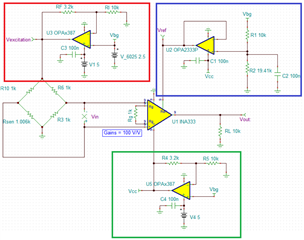
    a. The Wheatstone Bridge excitation voltage has to be a stable and bangap like voltage excitation source. It has to be stable. MAX17222 will not meet the requirements, especially the DAQ is sampled in 24bit accuracy, see the marked red box in the image above. 

    b. The orange box is a method to configure Vref at the mid point of 3.3Vdc. Again with 24bit ADC, I would recommend to use bandgap voltage reference to construct the ~1.65Vdc, e.g. REF34-Q1, REF3125, ref5025, ref5030, ref6025 etc.. 

    c. The INA333's output should have additional supporting circuit to interface with the ADS1220. For the best input coupling,  you should contact for the additional support from ADC team. 

    In addition, I need to know the following information. 

    1. What is the sensor application? What is excitation voltage and the sensor's operating range?

    2. Is this battery operating application?

    3. Does Wheatstone bridge require additional bridge balancing?

    4. What is operating frequency range? 

    5. Are there noise design requirements?

    Please let us know your requirement so we are able to help you to improve the design. 

    Best,

    Raymond

  • Hello Raymond,

    Please see response from my customer:

    a. Can you tell me in short why MAX17222 is not ideal? and what device should I look for inorder to boost DC, since my voltage supply is limited. I am only getting 1.8V and need to design system around it.

    b. I will look on those chips and see what I can find.(but again all this also depends on the boost converter because I need to use it since the 24bit adc works on 2.3V minimum)

    C. I will look up on that as well, thank you.

    1. I am using strain guage in bridge, again ex voltage depends on dc booster. The sensor operation range is +/-1.5% of its resistance which is 985-1015.

    2. this is wireless data aqusistion system(but my work is only till the value I get from ADC(also to calculate it in matlab))

    3 the bridge consist of two strain guage on same hand one for measruing strain and other to compensate for resistance.

    4. Can you please shed some light on this question? strain frequency?

    5. I have no instruction on noise requirements. so it's a blind spot for me right now.

    Regards,

    Renan

  • Hi Renan,

    Can you tell me in short why MAX17222 is not ideal?

    Raymond has already answered your question: The supply voltage of bridge must be clean, stable and noise-free. But when you have a look into the datasheet of MAX17222 you will notice that Vout is not clean and noise-free, because this chip is a DC/DC switcher producing lots of switching noise, as DC/DC switchers all do.

    And the output voltage of MAX17222 is not stable at all. There are even no specifications of temperature drift and long term drift in the datasheet. So unless you use the method of ratiometric measurement which can cancel errors of the bridge voltage to some degree the MAX1722 isn't suited at all to work in combination with a 24bit ADC. The bridge's voltage would need to be as precise as your 24bit ADC. With the MAX17222 or another DC/DC switcher you would fully ruin the 24bit precision.

    Kai

  • Hi Renan,

    What is the maximum current rating in 1.8V power source? If 1.8Vdc is only available power source, you will need boost converter to increase the voltage, but we may have to find a converter that has low noise ripple and stable converter.

    As Kai pointed out, your system's noise is determined by the 24bit ADC. Assume you are working with 3.3Vdc, and the ADS1220 has an effective 24 bit in performance. The system noise ripple should be less than 3.3V/2^(24-2.7) = 1.28 uV (assume the effective resolution will be better than the peak-to-peak resolution by 2.7 bits). Please consult with our ADC support team for further information. Maybe the application does not require 24 bit solution ADC per the design.  

    Can you upload the 985-1015's strain gauge datasheet? I did not find the part number readily. 

    Best,

    Raymond

  • Hello Kai and Raymond,

    Please see response from my customer:

    Ok I understand the shortcoming of MAX17222 booster now thank you. Lets assume for now that I have overcome the DC booster problem and( right now I am using a 3.3 supply from launchpad(msp430f5529) to perform circuit development) After taking your advice in the account I will invest in precision voltage source(which I will look for stability) and power it from launchpad during development and testing if its fine?

    Well you are quite right to assume that I don't need 24 bit of resolution as per expericnce of my colleague for my application( my thinking behind selection this adc was to have room for noise trimming and signal conditioning if needed after gathering data) .

    Ah yes the name of the guage is EK0-6-125AC-10C/W
    docs.micro-measurements.com/

    I am using 1000 ohm gauge of series EK with strain range of +/-1,5%.

    Can you please recommend me any precision voltage source that can be powerd from launchpad ? I have seen that the voltage output from board directly had ripples as well in oscilloscope.

    Regards,

    Renan

  • Hi Renan.

    Here is what I would suggest the design approach. I need additional information before I can provide you with a simulation. 

    1. How is the 1.8Vdc +/-X, and I need to know min and max of X value. What is current rating in 1.8Vdc?

    2. 1000 ohm gauge of series EK with strain range of +/-1,5%. Does the application require to work in both compression and tension mode. In other words, the strain gauge may have to swing from 985Ω to 1015Ω

    3. You need to find a boost converter that can boost from 1.8V to 4 to 5V range. I did not spend a great deal to find these boost converter. Perhaps you may find a better one. Switching frequency up to 500kHz is ok, and fix voltage converter may be acceptable, but you will need to check other noise specification. 

    https://www.ti.com/power-management/non-isolated-dc-dc-switching-regulators/step-up-boost/boost-converters-integrated-switch/products.html#p238min=0.3;1.8&p238max=1.8;75&p634min=-25;5&p634max=5;84&p212max=64;100&sort=p238max;asc

    The design approach is the follows. 

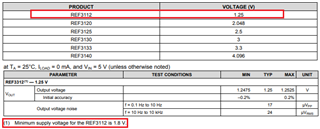
    a. Use 1.8Vdc to create of a stable reference 1.25V, say using REF3112. 

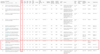
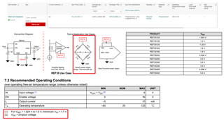
    Here is another new voltage reference you may consider - REF35, and it is low cost. 

    b. Use 1.8Vdc to create 4 to 5Vdc for a general purpose power rail, say to supply power rail to OPA333 or similar. The boost converter needs to be low noise. 

    c. Use 1.25V for INA333's Vref;

    d. Use 1.25Vdc to create excitation voltage via an op amp, say Vexcitation = 3.3V. The the excitation current for Wheatstone bridge is approx. 3.3V/500Ω =6.6mA. 

    e. Use 1.25Vdc to generate the additional voltage to drive ADC and/or MCU. 

    I need the above information and please let me know if this approach is acceptable. 

    Best,

    Raymond

  • Hello Raymond,

    Please see my customer response below:

    ok I reconfirmed with my project lead and he said it would be nice if I could take <= 1mW but its not much of an issue here.
    the task is based on unknow strain state in different structure with unknow directions so I a mtaking inaccount of both compression and tension henceI need the ina333 to midsupply.
    On finding booster converter I would like to ask you one more question: there is no mention of noise in the data sheet of your proposed converter(what specific thing should I be looking for in terms of relating to the performance of 24bit adc with noise of the converter(which electrical characteristic defines or give idea about noise))

    Can you also explain me what does point D and E in your proposed design really mean? My question regarding in terms of noise in above reply is to find a booster converter outside TI as well since all I see in the texas instruments website is out of stock due to chip shortage(no offence intended)

    Regards,

    Renan

  • Hi Renan,

    you can use the MAX17222 to generate a high auxiliary supply voltage from which you precisely produce the necessary lower supply voltages, for instance in the way suggested by Raymond. But you must not drive the bridge and the instrumentation amplfiers directly with the very noisy output voltage of MAX17222.

    Also, you should add low pass filtering in form of a Pi-filter at the output of MAX17222 to remove the nasty ripple. At the input of MAX1722 another Pi-filter can make sense to prevent the switcher noise from spreading and contaminating the ambient with EMI.

    Kai

  • Hi Renan,

    he said it would be nice if I could take <= 1mW but its not much of an issue here.

    Could you explain what <=1mW refers to?

    there is no mention of noise in the data sheet...

    Could you post the question to BMC-BCS team? I know that linear LDO has the noise specification. The boost converter may not pose the specification because of it is a variable depending on the switching frequency, inductor, capacitors and load in the circuit. I think that you are likely looking for low power, high efficient boost converter from 1.8V to 4-5V range. 

    Can you also explain me what does point D and E in your proposed design really mean?

    The strain gauge sensor is 1kΩ type, and the calculated current should be 3.3V/1kΩ = 3.3mA, not 6.6mA. (2kΩ||2kΩ). 

    If you have onboard precision reference voltage, you may use the external voltage reference for the required reference in ADC. The external voltage reference is typically more precise than the internal voltage reference in ADC in general (e.g. the ones that I posted in the reply).

    I see that Kai has replied. If you adapt the suggested design approach, the selections of boost converter is not very critical, as long as it will meet your power requirements (I think that you should select our converter, if possible). The purpose of the boost converter to boost the input voltage to 4-5Vdc, where you can use the boosted voltage to op amp's rails on the board. In other words, use op amps as voltage regulator to design the application (lower the switching ripple voltage). 

    If you have additional questions, please let us know.  

    Best,

    Raymond 

  • Hello Raymond,

    Please see response from my customer:

    I found some chip still availble from mouser, please tell me if i have made mistake in selection of those chips.
    OPA333AMDCKREP and REF6250IDGKT, to use at refernce of ina333 and also to use them as voltage source as suggested. of course i will do about PI filter before and adter max1222 if need( also use max1222 if need). also I would like to know what filters i should use after ina333 output( is Capacitive load drive = 500 pF) should this capactiance be of concern?

    Regards,

    Renan

  • Hi Renan,

    please tell me if i have made mistake in selection of those chips.
    OPA333AMDCKREP and REF6250IDGKT, to use at refernce of ina333 and also to use them as voltage source as suggested

    Please show your updated schematic to be able to help.

    also I would like to know what filters i should use after ina333 output( is Capacitive load drive = 500 pF) should this capactiance be of concern?

    The datasheet of ADS1220 discusses the input filter (= output filter of INA333) in every detail. See section 9.2.1. And if you select RF1=RF2=1k, there's no need to worry about the capacitive load at the output of INA333, because RF1 and RF2 not only serve as filtering resistors but also as isolation resistors effectively isolating any capacitive load from the output of INA333.

    Kai

  • Hi Renan, 

    Please see Kai's reply about the INA333's output. 

    Regarding to the input stage, here is an example. 

    INA333 + 24bit ADC 07182022.TSC

    Since you are selecting 2.5Vbandgap reference, OPA387 may be acceptable. If you select Vbg of 1.25Vref or similar, you may use LPV821 or similar zero drift op amp, which it has higher output current to drive Wheatstone bridge and INA333 at 3.3Vdc. 

    https://www.ti.com/amplifier-circuit/op-amps/precision/products.html#p2192=Zero%20Drift&sort=p1261max;asc

    If you have additional questions, please let us know. 

    Best,

    Raymond

  • Hello Kai,

    Please see my customer response:

    Here is the schematics( i have tried to follow manual and Raymond's recommendation of passive components). I will follow your advice on adding 1k resistors at input of ADS1220( ihave some other adc problems to deal with right now so) Thank you.

    3 ina333 and 1 ads1220 with ref62 and opa33.zip

    Hello Raymond,

    Please see my customer response,

    I do not understand your suggestion here since I am using OPA333 at per the datasheet(of INA333) and your advice. I have included the schematics updated which includes OPA333 and REF62. I haven't yet removed MAX17222 as booster since as per your suggestion I can use reference REF62 as voltage source as well? I will add PI filter before and after the MAX17222(as per Kai's advice) and connect the output to REF62 and use output of ref62 as voltage source and also as reference for ads1220.(is it good to do that?)

    Now I have included OPA333 to voltage divider for reference on INA333.

    Regards,

    Renan

  • Hi Renan,

    this is still not what Raymond has suggested in his last schematic. Every 5V you see in his schematic is supplied by the heavily low pass filtered output of MAX17222 (or any other switcher you need because of your only 1.8V supply voltage).

    The bridge, on the other hand, MUST NOT be supplied by the MAX17222 (filtered or not), because its output voltage is highly unstable and will totall ruin the precicion.

    Because of that the bridge and the INA333 are powered by the additional OPAmps U4 and U5. These OPAmps can suppress the output voltage fluctuations of the (heavily low pass filtered!) MAX17222 and provide ultra stable supply voltages derived from the REF6250.

    Kai

  • Hi Renan,

    Please see Kai's comments. 

    1. The Wheatstone bridge required 3.3Vdc @3.3mA minimum, stable, low noise, low drift excitation voltage, OPA333 is barely able to source the voltage and current adequately, but it is not a good option over temperature. I picked OPA387 or LPV821 (maybe). You use reference voltage 2.5V or 1.25V to create 3.3Vdc stable voltage source. 

    2. The same reason is used to power for INA333, In used OPA387 as well, since it can source adequate current @3.3V. 

    3. The onboard 5Vdc may be generated from MAX17222 + pi filter + LPF (if necessary)

    4. Vref of 1.25V or 2.5V is generated from 5Vdc (MAX17222) to the Vref.  

    5. The 24bit ADC or similar may be powered by from one of low noise, stable voltage source (say from step 3). I do not know what current is needed, but you should be able to figure it out. 

    If you have additional questions, please let us know. 

    Best,

    Raymond

  • Hi Renan,

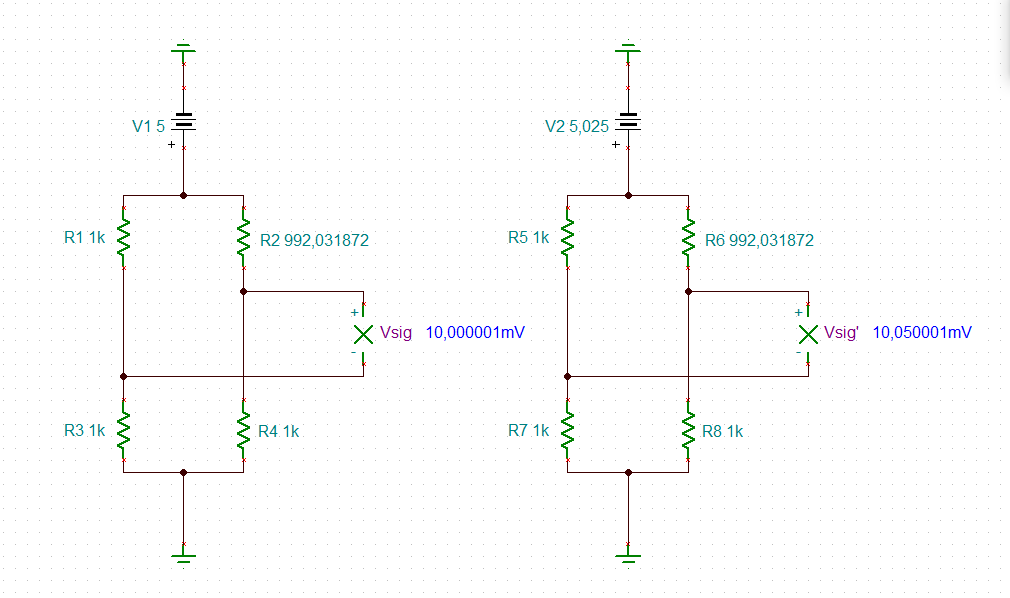
    to demonstrate how much the supply voltage of bridge can ruin the precision, see this example:

    Assume your bridge generates a signal of exactly 10.00mV with a supply voltage of bridge of 5.000V. This situation is shown on the left side in the below simulation.

    No assume that the same bridge with exactly the same stimulation sees a supply voltage of bridge of 5.025V, which deviates from 5.000V by 5%. Then the output voltage of bridge is no longer 10.00mV but 10.05mV. See the right side of simulation. This means an error of 0.05mV.

    An ADC with a LSB of 0.05mV and having 10.00mV / 0.05mV = 200 steps would create exactly the same error. An ADC with 200 steps is a 7.6bit ADC. So, from this moment on your 24bit ADC is only as exact as a 7.6bit ADC. You have lost more than 16bit of your 24bit ADC and this only because the supply voltage of bridge is drifting. 

    This simple simulation clearly demonstrates that the supply voltage of bridge must be extremely stable when you plan a high precision. You can very easily calculate how precise the supply voltage of bridge must be for a certain wished precision. This is no rocket science.

    renan_ina333.TSC

    Kai

  • Hello Raymond and Kai,

    Please see the update from my customer:

    sorry to reopen this matter. I believed that i had found the solution but I need to ask a really basic question here. the cirucit provided by Raymond consisting of two opax387 and one opa333, how can i expand it for three bridges here. Do I have to implement such circuit accross all three bridges or can i just connect all three bridge and ina333 parallely with the opax387 and opa333 setup?

    Regards,

    Renan

  • Hi Renan,

    When I picked the op amp components and demonstrated as an example, but I did not consider the cost. We have other cost optimized op amp choices, we can modify the circuit and meet your requirements in cost and performance etc.. 

    Since you have three Wheatstone bridge in the application, we may consider a different approach to design the requirements. 

    1. You may consider to use low noise and low drop out LDO to substitute the 3.3V shown in green block. 

    2. In the marked red block, OPA387 may be able to source 3x3.3mAdc in current in practice, but I would not recommend the tie all three sensors in one OPA387. All three transducers should have its own independent excitation voltage. For instance, if one sensor is gone bad, it will affect other two sensors, which are not considered a good design approach. 

    3. In the marked blue block, the same working logic may be applied. We may use TLV333 or TLV2333 to reduce the total cost. My recommendation is to keep all three transducer as independent as possible.   

    Since I do not know the customer's design requirements and the sensor failure criteria or requirements in the design, I am unable to recommend the best compromises. There are pros and cons in the above design approaches, which are typically driven by the application and design requirements. 

    Best,

    Raymond 

  • Hello Raymond,

    Please see my customer response below:

    I am terribly sorry to not mention this important detail about it. I am only looking for experimental design hence its is not a finished product. What I aimed for is to get values of strain gauge from those three bridges in order to calculate DELTA rossette strain. Hence the sensor failure rate is not much of an issue here. So how do I proceed here. I also have one question: Lets assume that I am taking output from a singular opa387 design at per point 2 and if one of the wheatstone bridge gets unbalanced that is strain guage output changes from 1000ohm to 1015 ohms during strained state. Will this affect output of other two bridges in any sense?

    This project is just on its experimental state, if everything works fine from using all three bridges and all three ina333 from single design proposed by Raymond then all I have to worry about is temperature because this whole setup will be going into oven and hence I will be using full range of temperature of these components -20° C to 120°C..

    Regards,

    Renan

  • Hi Renan,

    Lets assume that I am taking output from a singular opa387 design at per point 2 and if one of the wheatstone bridge gets unbalanced that is strain guage output changes from 1000ohm to 1015 ohms during strained state. Will this affect output of other two bridges in any sense?

    In the red block, OPA387 is driving an equivalent 3 kΩ resistors in parallel or driving approx 9.9mA or so @3.3Vdc. It may work at 25C for all three transducers, if Wheatstone bridge is using 1kΩ strain gauge sensor (assumed other balanced resistors are 1kΩ type). OPA387 will dissipate power at approx. (5V -3.3V)*10mA = 22mW. Even the strain gauge are unbalanced, it should not affect the OPA387's 3.3V's output, which it should be stable at 25C. 

    In the blue block, the OPA333P should be able to source or sink Vref = 1.65V for three INA333 as well. 

    In the green block, I would use LDO instead. If the INA333's output is driving a very light load, then the OPA387 circuit may be able to drive all 3 of INA333 at 25C. You may have to check the OPA387's driving current is going to be. If the OPA387's sourcing current is over 20mA range @3.3V at 25C, I would evaluate the droop voltage at the output OPA387. My guess is that a single OPA387 may drive up to 2 of INA333 (light load), but I am not certain about all three at the same time.

    In all cases, we are using precision op amps as precision voltage regulators; the concerns are about the heat dissipation and amount of current that the op amps are able to source/sink for the application. If the op amps remains cool for the worst case of temperature testing and the output voltage does not droop, then you may use these as the voltage regulators.   

    If you have additional questions, please let me know. 

    Best,

    Raymond

  • Hello Raymond,

    Please see our customer response below:

    I have taken OPA4387 which has 4 channels, hence I can drive 3 bridges simultaneously? I am talking about red block and green block as well.

    I will have 3 opa333 hence blue block is solved as well.

    I also have one more question here:
    How should I place positive reference and power supply of ADS1220 here? Since what I read was to keep reference and power source as same as bridge and ina333 power supply.

    Regards,

    Renan

  • Hi Renan,

    I have taken OPA4387 which has 4 channels, hence I can drive 3 bridges simultaneously? I am talking about red block and green block as well.

    It is likely that you are unable to drive OPA4387 in 4 channels. I do not know how much power each INA333 is going to source. Since the application is using OPA4387 as voltage regulator, it is not good ideas to dissipate the power in a single IC. Quad package OPA4387 is not designed for this type of application. You will be better off the power these individually with different op amps, especially you want to guarantee the minimum of 22-23bits out of 24 bit ADC. 

    How should I place positive reference and power supply of ADS1220 here? Since what I read was to keep reference and power source as same as bridge and ina333 power supply.

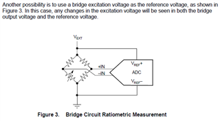
    I think that you are referring to ratiometric ADC measurement. Please see the attached links below. For further support, you should contact ADC team for the recommendation. 

    lpvo.fe.uni-lj.si/.../sbaa110_Understanding_Ratiometric_Conversions.pdf

    https://static5.arrow.com/pdfs/2013/11/24/3/19/23/744/txn_/manual/slau520.pdf

    Best,

    Raymond

  • Hello Raymond,

    Please see our customer response below:

    Ok, if thats the case without trying to sound stubborn, can we drive single INA333 + supply and bridge supply from single OPA4387(single channel(bridge supply plus ina positive supply) or dual channel( seperate channel from single OPA4387 for bridge supply and INA333) configuration)?


    Since I am not using differential measurement directly from bridge to adc, we have INA333 in between., if you approve to above mentioned configuration how do you propose the placement of +/-VREF since we are using separate voltage source(opa4387) for each bridge and ina333? Please tell me if this is the question to be asked from ADC team.

    Regards,

    Renan

  • Hi Renan,

    Ok, if thats the case without trying to sound stubborn, can we drive single INA333 + supply and bridge supply from single OPA4387(single channel(bridge supply plus ina positive supply)

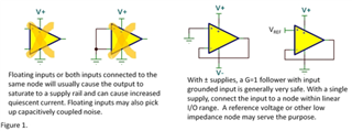
    This may be ok, if the INA333's load is light. Here is why. You have an unused op amp channel and please make sure that it is placed in a linear operating mode (do not let is float or operating in saturation mode). 

    A single Wheatstone bride (with 1kΩ transducer type) will draw current approx. 3.3mA with Vexct = 3.3V

    Vref = 1.65V for INA333's reference may source/sink negligible amount of current. 

    INA333 under a single supply of 3.3V may draw a few mA under light load (assumed a light load condition). 

    or dual channel( seperate channel from single OPA4387 for bridge supply and INA333) configuration)?

    This may work as well. 

    if you approve to above mentioned configuration how do you propose the placement of +/-VREF since we are using separate voltage source(opa4387) for each bridge and ina333?

    There are several design approach for this. 

    1. You may pick one Vexcitation as the represented one for the ratiometric voltage reference tracking (assume other two are equal). 

    2.  You may average all three Vexcitation voltages and use the average as the ratiometric voltage reference. 

    Method 1 is simpler. 

    You should contact ADC supporting team anyway. Perhaps they have a better option for the ratiometric tracking. In addition, the INA333 output connection to ADC is not a direct interface in ADS1220. You need to get a recommendation from the supporting team.   

    Best,

    Raymond

  • Hello Raymond,

    Please see my customer response below:

    Thank you Raymond,

    I have two questions here,

    should i ground every other channel which is not being used in OPA4387? not to let the channel float that means it should be grounded, right? what does it means to have them in linear operation mode?


    I haven't had my hands on those components yet but I saw that you added 19.41k(R2) resistor beding OPA333 in voltage divider, should it be 10k or does the impedance of input of OPA333 will affect the output of voltage divider here?


    I have contacted ADC team and they will be advising me on further queries but can you keep this thread open for a little longer in case i have to come back?

    Regards,

    Renan

  • Hi Renan,

    should i ground every other channel which is not being used in OPA4387? not to let the channel float that means it should be grounded, right? what does it means to have them in linear operation mode?

    I am enclosing two references for the unused op amp configuration. 

    In  an op amp linear operation mode, the output signal vs. input signal shall follow the following equation --> Vout = Gain * (Vin+ - Vin-). If you want to have a detail of the explanation, please let us know. 

    https://e2e.ti.com/blogs_/archives/b/thesignal/posts/the-unused-op-amp-what-to-do

    https://www.ti.com/lit/an/sboa204a/sboa204a.pdf?ts=1659886349437

    In the case of OPA387, the input signal needs to be kept within the Vcm range over temperature. Grounding the input voltage or higher within the Vcm range of unused of OPA387 is acceptable (to keep the unused op amp in a linear region). 

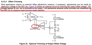
    I haven't had my hands on those components yet but I saw that you added 19.41k(R2) resistor beding OPA333 in voltage divider, should it be 10k or does the impedance of input of OPA333 will affect the output of voltage divider here?

    The input of OPA333 may use lower resistor values to construct a designed voltage divider. The low impedance node has to be placed at Vref circled below. The output impedance of an op amp is a low impedance node. Op amp has high input impedance, so it is not important to use high resistor values, unless the resistor's thermal noises become dominate at the noise of the buffer operation in OPA333.  

    If you have additional questions, please let me know. 

    Best,

    Raymond