


Part Number: OPA991
Hi Team,
Good day!
Our customer found a significant mistake in the datasheet. I have post their full details of inquiry below.
I have recently purchased OPA991TIDCKR and fitted to a development PCB using the PCB layout as designed on line for DesignSpark PCB. The layout used is in accordance with the diagram Fig 5-2 on page 4 of the data sheet for the DCK 5-pin SC70 package. The actual device marking is 1HB so corresponds with the OPA991IDCKR data shown in the table for packing information on page 1 of the Addendum. However, upon assembly of the circuit and subsequent testing, it appears the pinout of the part supplied is actually as shown in Fig 5-1 on page 4. The Addendum-Page 1 table shows there isn't an SC70 package in anything but the DCK version yet Fig 5-1 is also anotated as DCK and SC70. Can you please state exacly which pin out should apply to the DCK SC70 package and, if it is that shown in Fig 5-1 (as testing says it does), then why is it shown in the data sheet as being that in Fig 5-2? .But as far as they tested, this layout information is wrong and it should be like the below. #1 and #4 are inverted.
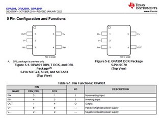
Could you please check if the customer is correct?
And if they are correct, could you please update the datasheet as soon as possible?
Best regards,
Jonathan

