This thread has been locked.

If you have a related question, please click the "Ask a related question" button in the top right corner. The newly created question will be automatically linked to this question.

THS4631DDAEVM: Opamp input problem

Part Number: THS4631DDAEVM
Other Parts Discussed in Thread: THS4631

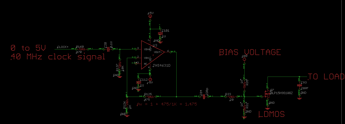
In the circuit below, I send short trains of pulses (0 to 5V) at 40MHz into the CLOCK+ pin.

The signal looks good at this point. However, on pin 3, the clock signal begin to look crazy as I increase VPP (my DC bias voltage on the LDMOS)
When Vpp = 1.5V, the voltage at pin 3 starts randomly shifting up and down with some dc offset, and sometimes the clock signal disappears for  short time, and then turns back on?

I can't understand what is going on, I would think the input impedance at pin 3 would not be changing so I don't understand how the signal at pin 3 can suddenly drastically change.

Anyone have any insight?

  • Hi Craig,

    does it work properly when you remove the LDMOS so that only C84, R23, R31 and R35 are present in the circuit?

    Also, what happens when you take a fresh THS4631?

    Kai

  • Hi Kai,

        Yes, if I remove the LDMOS, the output signal is exactly what I would expect between R35 and R31,

    this worked for all bias levels (Vpp = 0 to 3.3 volts).

    What does this mean, am I overloading the opamp, so its failing?

    -Thanks,

         Craig

  • Hi Craig,

    I have no experience with LDMOS, unfortunately. It can be that the output of OPAmp does not like the input impedance of LDMOS. Or, stimulating the gate of LDMOS by the OPAmp can have a consequence which feedbacks to the OPAmp and destabilizes it. Think of unwanted coupling via a common supply voltage or via signal ground.

    Does changing the load of LDMOS show any impact on the performance of OPAmp?

    What is the input impedance of LDMOS? Is there an equivalent circuit of the LDMOS you can share? Does taking a fresh LDMOS and/or OPAmp help?

    Does probing with a multi-channel scope show any coupling effects, when you probe the THS4631 and LDMOS at the same time? Can you also probe the supply and auxiliary voltages?

    Kai

  • Hello Craig,

      It looks like you followed the correct procedure for resistor at the output to "isolate" the load capacitance.

      On top of the Kai's suggestions: (test for each step below in order)

    1. Keep LDMOS but remove connection for anything after (C93 and To Load) 
    2. Solder a 8.2pF capacitor right on top of RF (R125). This amplifier seems to be slightly decompensated as suggested by the peaking in the datasheet figures. 
    3. Increase isolation resistor (R23) from 20 to 100 Ohms. The LDMOS looks like has a max of 40pF, and datasheet does state 20 ohm resistor, but from a quick sim it seems like it does need the additional increase. 

    Thank you,

    Sima