This thread has been locked.

If you have a related question, please click the "Ask a related question" button in the top right corner. The newly created question will be automatically linked to this question.

INA209: INA209 - Fail to access on Address involving SCL/SDA

Part Number: INA209

Hello,

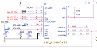
I'm using 10 x INA209 in my design.

F= 100KHz

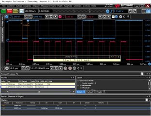
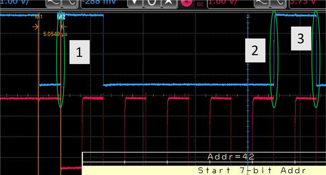
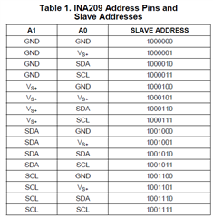
I'm having problem of accessing the ones which are configured to I2C ADDR by strappin A1 A0 to SDA / SCL (for exampleL addr 0x42 (A1=GND, A0=SDA))
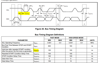
The DS says :

"The state of pins A0 and A1 requires a value for the register pointer.
is sampled on every bus communication and should Writing to a register begins with the first byte
be set before any activity on the interface occurs"

Can you please expalin what is the point in time where the A1 A0 Being sampled

Are there any timing restrictaion for SCL / SDA in order for the address to be captured correctly?

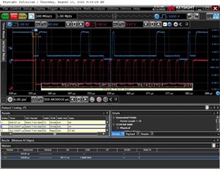
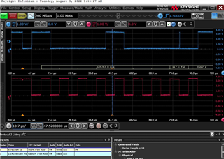
Adding picture for accessing 0x42 - No Ack

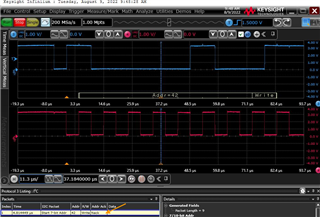
Adding picture for accessing 0x44 - with Ack

Thanks

Dror

  • Hello Dror,

    Are you pulling the address pins A0, A1 with resistances >0-Ω?

    Every time the primary host controller initiates a START condition, the INA209 will read the state of A0 and A1 to determine its secondary address. This can pose a problem with devices that have A0/A1 pulled up to SDA since a START is generated by pulling SDA low and depending upon board parasitics there can be a chance that SDA goes LOW before device has even determined the Ax state, thus it will not acknowledge at the end of transmission. This issue is made worse if there is resistance/inductance in between MCU SDA pin and INA209 address pin.

    If it is possible try reducing SDA load capacitance and any trace resistance/inductance in between A0 and SDA and/or SDA of host and SDA of INA209. Reducing pull-up resistance can also help. If these do not work and you cannot avoid pulling an address pin up to SDA, then you will have to increase the START hold time (t_HDSTA) of the MCU up to an additional 100ns to ensure that INA209 determines its secondary address before the end of the START condition (start of 1st SCL clock).

    Hope this helps. Please post back with any other questions and/or updates.

    Sincerely,

    Peter

  • Hello Peter,

    The resistors between A0/A1 to SCL/SDA/GND/VCC are 0 Ohm 

    Screen shot of the schematic is below


    I'm adding  2 scope capture:

    1. Transaction made by USB to FTDI (I2C) chip (FT4222HQ) - where the INA send ACK. (FTDI works in 400K)

    2. Transaction made by out chip  (works in 100K) - where the INA din't send ACK

    In both cases the Start time is much beyond 100n...

    Picture #1:

    Picture #2:

    Can you please specify what is exactly the point of A0/A1 capture during the "Start condition" ?

    I do not understand why we fail with our chip?

    Dror

  • Hey Dror,

    Thank you for sending the scope shots. You are right that the start hold times are valid. However, you could be facing a problem with the data hold times (HHDAT) after the start condition, and this could also be causing the NACK.

    In you second image, I circle three instances where the data hold times are essentially 0ns (or less, hard to say). All three instances show different timing behavior when compared to the first image. While we list 0ns has a valid data hold time, it is best practice to incorporate some margin (~10ns) to account board parasitic impedances.

    At instance "1", this is not technically a data hold time as shown in the timing diagram because it occurs before first SCL pulse; however, it is indicating that SDA is going to move once SCL falls one half-period before the corresponding SCL pulse. This essentially means you are maxing out the data set up time and minimizing the data hold time. You could try just increasing the hold time here (the time from SCL fall to SDA rise after start condition, if possible) and see if this fixes the problem, but most likely you will have to do the same for all data hold times.

    In instance "2", SDA rises at the same time SCL falls. Increasing data hold time here means putting ~10ns of time in between SCL fall and SDA rise.

    In instance "3", SDA falls at the same time SCL falls. Increasing data hold time here means putting ~10ns of time in between SCL fall and SDA fall. 

    Hope this makes sense.

    Sincerely,

    Peter

  • Hi Peter,

    T(HDDAT) is specified as 0nSec min and seems like the device must have as you said ~10nSec.

    This is a typo in the DS isn't it?

    BTW: We added RC delay on the A0 Series resistor (changing the 0 Ohm to 1K and added 100pF to GND) this resolve the issue but required a patch on my board.

    Next time - I will not use Address which invovle with SDA...

  • Hey Dror,

    The 0ns t_HDDAT is not a typo. The device was characterized with this timing; however, setting t_HDDAT at this time can be marginal given that there can a longer delay if board parasitics are not accounted for, thus I recommend just a few ns extra to provide plenty of margin. More importantly, the 0ns hold time becomes problematic when pulling an address pin to SDA, and this is a typo and we are working to mention this in datasheet. We apologize for the inconvenience.

    So increasing data hold time is one way to fix this issue. It seems placing a RC at A0 is another way, although let me look into whether these value can be optimized further for robustness if you cannot increase data hold time in your system.

    Sincerely,

    Peter