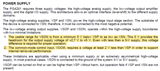
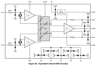
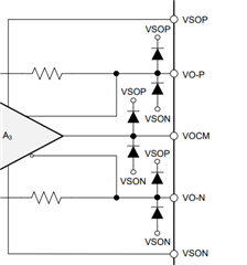
Part Number: PGA281
Hi, team!
I have a question about PGA281 power up sequence question.
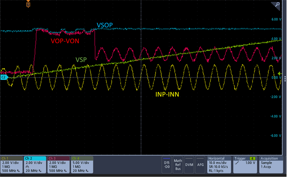
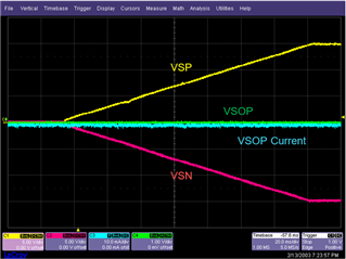
I tested PGA281EVM and tried to give 2.6V to IN-N and 5.2V to IN-P, gain=1(G4:G0=00011), VOCM=2.5V, and wanted to get 1.2V ~3.8 on VON and VOP, with VSP=15V, VSN=-15V, VSOP=VDD=5V.But when I power up PGA281, it occurs some question.
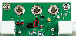
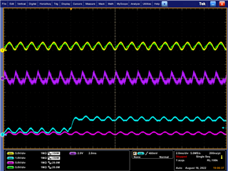
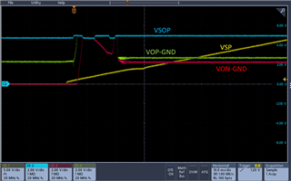
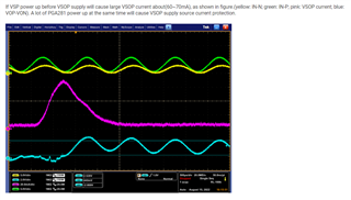
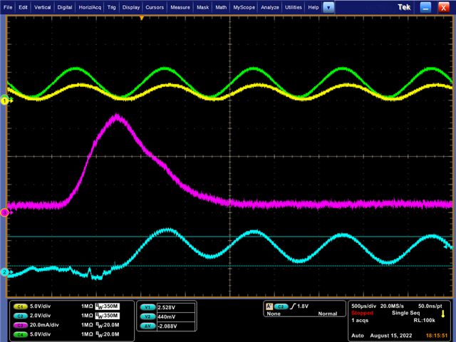
If VSP power up before VSOP supply will cause large VSOP current about(60~70mA), as shown in figure.(yellow: IN-N; green: IN-P; pink: VSOP current; blue: VOP-VON). A lot of PGA281 power up at the same time will cause VSOP supply source current protection.
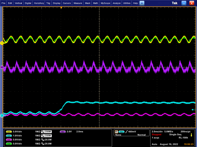
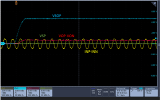
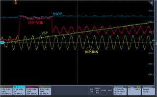
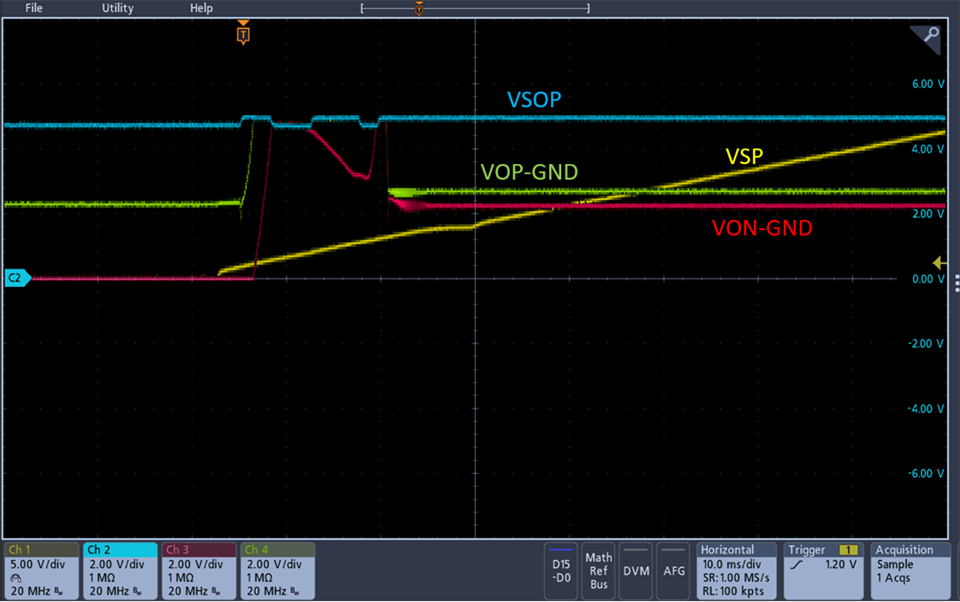
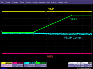
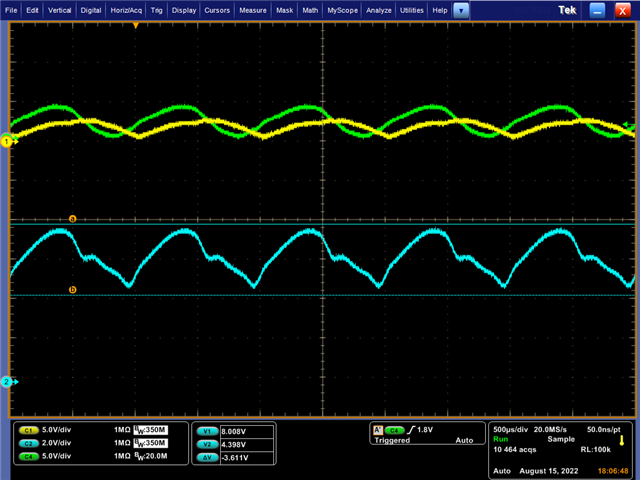
If VSOP power up before VSP will cause PGA281 output range over ADC input range, as shown in figure. It maybe reduce device ADC life.
Could anyone help me solve this problem for both situations and explain the reason?