This thread has been locked.

If you have a related question, please click the "Ask a related question" button in the top right corner. The newly created question will be automatically linked to this question.

PGA308: How to read the internal RAM data (CFG2) out from DOUT pin (No.1).

Part Number: PGA308
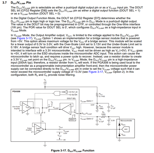
Other Parts Discussed in Thread: TRS202

Hello guys,

One of my customers is evaluating PGA308 on their own board for their new products.
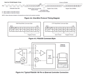
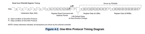
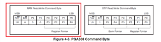
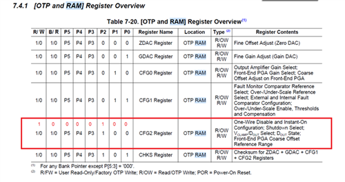
They want to read "CFG2" RAM data out from DOUT pin (No.1) using "1W" pin.

Could you please tell me how to read the data out? 

Your reply would be much appreciated.

Best regards,
Kazuya.

  • Hi Kazuya,

    I understand you want to read data from the PGA308 CFG2 register using custom board.

    The PGA308 uses a one-wire communication protocol, where both the PGA308 register data and the read/write command data from your controller will be sent on the 1W pin.

    The Dout/Vclamp pin can be configured as a push/pull digital output (Dout Mode) by bit [D8] of the CFG2 register. In Dout Mode, the Dout pin can be driven logic high or logic low by bit [D7] of the CFG2 register. This function is similar to a digital general purpose output (GPO) pin and does not send serial register data.

    You may send and receive PGA308 register data using the 1W pin and one-wire communication protocol as described in section 4 (Detailed Digital Description) of the PGA308 User's Guide.

    Regards,

    Zach

  • Hi Kazuya-san,

    A couple of additional comments Regarding the One-Wire protocol:

    As Zach has mentioned, Figure 4-2 and Figure 4-3 on Section 4.4 Digital Interface of the PGA308 User Guide explains the One-Wire protocol used on the 1W to communicate with the PGA308 on page 54.

    All communication transactions start with an initialization byte (55h) transmitted by the external controller. The second byte is the command byte (Figure 4-3). 

    On the Command Byte, the MSB is the R/W bit. Use MSB='1' indicating a read command. The next bit is the B/R bit.  Use B/R = '0' for RAM access.  Table 7-21 on p.88 shows the OTP and RAM register overview.  To read the CFG2 RAM register use P[5:0]: 000100.


    Refer to Figure 5-8 for the PGA308 read algorithm on page 64 for more details.

    Please keep in mind, it is important to access the One-wire while the interface is active.  Depending on the standalone configuration and how the OTPs have been programmed, and the programmed OWD register settings, the one-wire may time out shortly after power-up.   This is especially true in three-terminal modules where the 1W pin is connected directly to VOUT.  Read in detail section 5.5 'Standalone Mode' and 'software lock mode', and refer to the details of figure 5-10 standalone algorithm.

    Thank you and Regards,

    Luis

  • Hi Luis, Zach,

    Thank you very much for your reply.

    They wrote the following data to CFG2 register. 
    D15:OWD = "1"
    D14:OWD OFF = "0"
    D13:DIS OUT = "0"
    D12:NOW = "0"
    D11:COSVR[1] ="1" 
    D10:COSVR[0] ="1" 
    D9:  RFB = "0"
    D8:  DOUT SEL = "1"
    D7:  DOUT = "1"
    D6:  SD = "0" 
    D5~D0: RFB - "00000b"

    Are these data correct to read data out from DOUT terminal of PGA308?

    Thank you again and best regards,
    Kazuya.

  • Hi Luis,

    Could I ask you an additional question as the below?

    The customer want to write register data to PGA308 and read register data from the device by PC through RS232C transceiver like TRS202.

    TRS202
    https://www.ti.com/jp/lit/ds/symlink/trs202.pdf

    Their connection between PC, TRS202 and PGA308 is the follow.

    PC                            TRS202                TRS202                 PGA308
    Tx (RS232C port) -> RIN2(No.8)     ->  ROUT2(No.7) ->   1W(No.2)
    Rx(RS232C port) <-  DOUT2(No.7) <- DIN2(No.10)   <-    DOUT/VCLAMP(No.1)

    They want to read register data out from DOUT/VCLAMP terminal of PGA308.
    Also they want that the internal open-drain MOSFET connected to 1W isn't turned on because TRS202 ROUT2 (output terminal) is connected to 1W.

    They want to know what data should be written to CFG2 register?
    Could you please give me your answer for them?

    Thank you and best regards,
    Kazuya.   


  • HI Kazuya-san,

    Unfortunately, it is not possible to read register data from the DOUT/VCLAMP (No. 1) pin.  This pin is not part of the serial interface, and can only produce a static logic high or static logic low.

    The DOUT SEL bit (CFG2 Register [D8]) sets the DOUT/VCLAMP pin as either a digital output function (DOUT SEL = 1) or as a VCLAMP function (DOUT SEL = 0). In the Digital Output Function Mode, the DOUT bit (CFG2 Register [D7]) determines whether the DOUT/VCLAMP pin is logic high or logic low.

    Hence, the customer can only write or read register data through the 1W (pin2) One-Wire UART pin.

    Thank you,

    Luis

  • Hi Luis,

    Thank you very much for your reply.

    Could I ask you an additional question as the follow?
    Q. What is this function for? Is it just used as a general purpose output port?

    Thank you again and best regards,
    Kazuya.

  • H Kazuya-san,

    To answer the Customer question:

    What is this function for? Is it just used as a general purpose output port?

    Yes, the Customer is correct.  When configured as DOUT, the pin is used for general purpose static high /static low digital pin.  The original intent during the PGA308 product definition was to use the DOUT pin to control an external analog switch, so that the same PGA308 hardware module could be re-configured as either a voltage output or current output in the hardware, using an external analog switch to change the circuit configuration.

    Please refer to this previous E2E post regarding DOUT function:

     https://e2e.ti.com/support/amplifiers-group/amplifiers/f/amplifiers-forum/402048/inquiry-regarding-usage-of-dout-functionality-on-pga308

    However, in the majority of cases, Customer's use the VCLAMP/DOUT pin configured as VCLAMP pin to limit the output voltage, and avoid damaging a lower voltage input ADC during a fault condition.  See detailed below explanation of VCLAMP functionality from the PGA308 User's Guide on page 44:

    Thank you,

    Kind Regards,

    Luis 

  • Hi Luis,

    Thank you very much for your reply.

    I understood well and it is very helpful for the customer and me.

    Thank you again and best regards,
    Kazuya.

  • Hi Kazuya-san,

    Thank you,

    Kind Regards,

    Luis