This thread has been locked.

If you have a related question, please click the "Ask a related question" button in the top right corner. The newly created question will be automatically linked to this question.

OPA3S328EVM: OPA3S328EVM

Part Number: OPA3S328EVM
Other Parts Discussed in Thread: TINA-TI

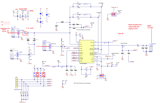
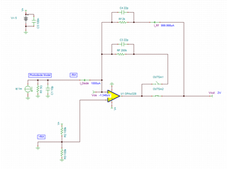
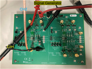
I have OPA3S328EVM board with me for testing, I am trying to simulate in-gas photodiode which has two ranges for my application 10uA - 1mA and 50uA - 5mA

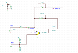
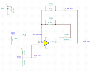
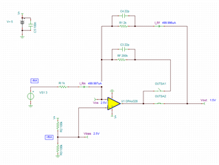
i am using the inbuilt resistor of 1K to convert voltage input into currrent using the vaiable voltage from external SMA connector from 500mV - 2V with selected gain of 2K using site 1.

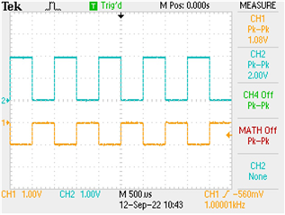
with 1V input, i should get 2V output correct? I am not able to read the correct output.

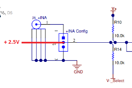
also supply ground and input connector ground should be same? right now i am connecting functional generator square wave to the input and 5V DC supply to  the V+ and supply ground to V-, and all the jumpers are placed accordingly

A1 low A2 shunt B1 low B2 shunt J11 & J17

Can you please provide the application example or details.

thank you


  • Hi Deepti,

    I understand you are using site 2 of the OPA3S328EVM and applying +1V to J17 labelled "-INA".

    Have you configured the "+INA" input at jumper J23? If this jumper is left open, the non-inverting input of the amplifier will be set to mid-supply by default.

    If you are applying 1V referenced to GND at -INA and +INA is referenced to 2.5V, the amplifier will attempt to output 5.5V which is outside of the supply range and the output will be railed at the positive supply.

    If the +INA is configured for GND reference (J23 shunted 2-3), this is essentially an inverting amplifier with a gain of -2k/1k = -2V/V.  If you are applying a +1V input referenced to GND at -INA and +INA is referenced to GND, the amplifier will attempt to output -2V which is outside the supply range and the output will be railed at negative supply.

    Please confirm the configuration of J23. If further support is needed, please provide oscilloscope capture of your input and output waveform and a photo of your test setup.

    Regards,

    Zach

  • Hi Zach,

    Thank you for replying.

    I am using Site 1 of the circuit

    -INA J4 pin 2 is connected to signal generator and Pin 3 is connected to Signal generator ground

    +INA J6 is jumpered pin 2 & 3

    J1connected to 5V and J2 connected to supply ground, V-left open and J11 shunt 2-3

    J16 shunt 1-2 for analog ground

    J8 is connected to scope.

    I will try using the non-inverting mode connecting J6 to input since the output voltge might be negative so it may not be able to read it.

    also supply ground and input ground are different, not sure if it affects my readings.

    I will capture the scope images and send you on Monday.

    Thank you for help!

  • Hi Deepti,

    when you power the OPAmp with a single supply voltage you must bias the +input of OPAmp with an auxiliary voltage of about middsupply (pseudoground). This is provided by the voltage divider R10/R14. As consequence the -input of OPAmp also sits at middsupply and you will need to AC couple the waveform generator. So insert a suited AC coupling capacitor between the output of waveform generator and R8.

    Alternatively you can power the OPAmp with a bipolar supply voltage and connect the +input of OPAmp to 0V. Then there's no need to AC couple the waveform generator.

    Kai

  • Hi Deepti,

    Thanks for the clarification, the information I gave above about biasing the non-inverting input (+INA) and violating the output voltage swing applies to site 1 as well.

    Is your signal generator capable of providing a negative input voltage? This will produce a positive output voltage in the inverting configuration and is closer to the transimpedance application you are attempting to simulate.

    If you are using an SMA cable to connect your signal generator to -INA (J4), your signal generator ground will be connected to the analog ground of the EVM through the SMA ground pins. You also have your jumpers configured so that the analog ground is connected to the supply ground (J2). To verify that input ground and supply ground are connected, you may use an ohmmeter to probe between J2 and the ground pins of SMA connector J4 (Be sure that the supplies and any inputs are powered off before probing with ohmmeter!).

    Regards,

    Zach

  • Hi Zach,

    Here are the picture and video of the testing i did, I Still gave square wave from signal generator with very less frequency of 1Hz,

    I did not connect input from input SMA, i connected the input only and not the ground through J18 connector. i used the supply ground only. 

    I also gavemidsupply 2.5V to +INA and power supply was 5V and ground, if i use 5V supply i should be able to use the full scale?

    input i varied from 1V-2.5V. the output was varying but it was not proportiona lto the input and it was saturating at 2.7V. may be because of midsupply?

    I need to test the range of input current 10uA - 5mA.

    for the full scalle of 5V, i might need external 4k-5k resistor, next set of test i am planning to do with second voltage supply to the input instread of signal generator.


  • Hi Deepti,

    I did not connect input from input SMA, i connected the input only and not the ground through J18 connector. i used the supply ground only. 

    I also gavemidsupply 2.5V to +INA and power supply was 5V and ground, if i use 5V supply i should be able to use the full scale?

    input i varied from 1V-2.5V. the output was varying but it was not proportiona lto the input and it was saturating at 2.7V. may be because of midsupply?

    I'm rather confused now. Please draw a schematic.

    Have you already tried AC coupling? Increase the frequency of signal, otherwise you will need a huge AC coupling cap.

    Kai

  • Sqaure wave with 0-1V input with 1MHz frequency, do i need coupling cap?

  • Please draw a schematic of what you are doing.

    Kai

  • Hi Deepti,

    I am unable to view the contents of your zip file. E2E allows you to copy and paste images directly into your reply as a .png file. In the future, please try copying and pasting your images into the reply, instead of using a zip file.

    Can you please clarify the following:

    I did not connect input from input SMA, i connected the input only and not the ground through J18 connector.

    In your previous response, you said:

    I am using Site 1 of the circuit

    -INA J4 pin 2 is connected to signal generator and Pin 3 is connected to Signal generator ground

    J18 is connected to -INA for site 2. Are you attempting to use site 2 now?

    You need to connect your signal generator ground to the ground of the OPA3s328EVM, otherwise you do not know what your input signal is referenced to. I believe the issue you are seeing is to due either connection, reference, or biasing of the input signal to the EVM. The proper biasing of your -INA input signal depends on how you have configured the +INA input at J6/J7 (site 1).

    You may refer to the following simulations for insight on proper input signal biasing.

    Please attempt one or both of these configurations using site 1 and provide scope-capture of input and output waveform. Ensure that signal generator ground is connected to EVM ground.

    Case 1: J7 shunt pins 2-3, +INA = GND.

    Input signal: square wave from 0V to -1V, f=1kHz.

    OPA3S328_+INA_GND.TSC

    Case 2: J7 shunt pins 1-2, J6 unconnected, +INA=2.5V (mid-supply).

    Input Signal: square wave from 2V to 3V, f=1kHz.

    OPA3S328_+INA_2.5V.TSC

    Regards,

    Zach

  • Thank you for your help and support, i am working with such low currents for the first time. before i design the proto board with in-Gas photodetector soldered on it, i wanted to understand how it works.

    Thank you Zac, 

    I will do the above tests on friday and send you the scope capture.

    the negative voltage may not work for my application

    case 2 seems more relavent, if i calculate the current with the internal resistor of 1K, with the innput voltage ranging from 2V-3V the current flowing to amplifier will be 2mA - 3mA 

    I used site 1 only Below is the schematics and picture, i am not able to attach the video here somehow.

    wires are directly connected to J5 for input and J7 for midsupply,  the analog ground @supply and input are internally connected, but i will connec tthe signal generator ground to the input

  • Hi Deepti,

    I am happy to help and looking forward to seeing your progress on Friday. Keep in mind that for a transimpedance amplifier (TIA), the input signal is a current source not a voltage source. Understanding the circuit's voltage bias and current flow is important for photodiode TIA.

    For example, in photodiode transimpedance applications, there is often a negative current with respect to the input. That is, current is pulled out of the input rather than forced in. This is why a negative input voltage across the input resistor (case 1) is useful because it generates a negative current with respect to the input, similar to the photodiode. See below.

    In your application you may choose to bias your photodiode to some value other than ground, but you must consider the current flow and how that effects the voltage at the output of the amplifier. I highly recommend using TINA-TI simulation tool to check voltage and current at various nodes to get further insight into the circuit. https://www.ti.com/tool/TINA-TI 

    One more thing... I see you are connecting a wire to J7 to set +INA bias at mid-supply. This is not necessary because if you leave J6 and J7 unconnected, the J7 pin 2 node will be set to mid-supply by voltage divider R10 and R14. However, if you choose to use external voltage source to set +INA bias voltage, make sure that your external voltage source ground is connected to the ground of the EVM as well.

    Regards,

    Zach

  • Hi Deepti,

    Let me clarify a couple more things.

    case 2 seems more relavent, if i calculate the current with the internal resistor of 1K, with the innput voltage ranging from 2V-3V the current flowing to amplifier will be 2mA - 3mA 

    This is incorrect. For case 2 the amplifier is biased to 2.5V. For 2V input, the current flowing into the input pin I_input = (2V-2.5V)/1kΩ = -500µA

    For 3V input, the current flowing into the input pin I_input = (3V-2.5V)/1kΩ = 500µA

    See below.

    Additionally, your schematic shows you are reading the output voltage with a DMM. The DMM output is an average value and does not give much insight on the waveform of an AC signal. When reading AC signals it is best to use an oscilloscope that can capture the waveform in detail whenever possible.

    Regards,

    Zach

  • Attached are the test results for case 1 with +INA grounded and input 0 to -1V

    Thank you,

    Deepti

  • Hi Deepti,

    I see we are making some progress. One thing I recommend is to always probe both the input and output waveform when debugging a circuit. Sometimes the input is not always as expected.

    Can you provide scope image of both the input and output waveform? Please provide an image of your test setup as well. You may use my test setup and scope image below as a reference.

    Regards,

    Zach

  • Hi Zach, 

    I am trying to add video which is not working, But i did the exact set up as above, but instead of connecting input ground directly to TP11 (analog ground) i did it through breadboard @ J4 pin 3 and J6 pin 2

    is the resistance of ground wires affecting the output?

  • Hi Deepti,

    No need to post a video. Just a couple clear images of your test setup and the input/output waveforms is good enough.

    is the resistance of ground wires affecting the output?

    It is not likely that resistance of jumper wires will be significant enough to cause an issue, however it is very likely that the resistance of the breadboard tracks (and other breadboard parasitics) could be an issue. Breadboards are a useful tool for building "quick and dirty" circuits, however you should avoid using them if possible especially for precision circuits.

    In this case, there are plenty of test points and ground connections available on the OPA3S328EVM so the breadboard is not necessary. Running your ground connections through a breadboard can only produce worse performance than the ground connections that are readily available on the EVM.

    For your next test I recommend leaving the breadboard at home and using the direct connections on the EVM. See the test setup shown in my previous post for reference.

    Regards,

    Zach