This thread has been locked.

If you have a related question, please click the "Ask a related question" button in the top right corner. The newly created question will be automatically linked to this question.

TL074: CMRR Circuit design

Part Number: TL074

Hi 

I'm Joe GZ FAE and my account is SAJ.

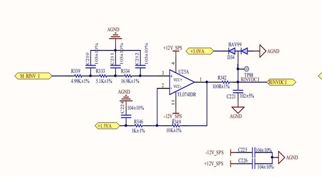
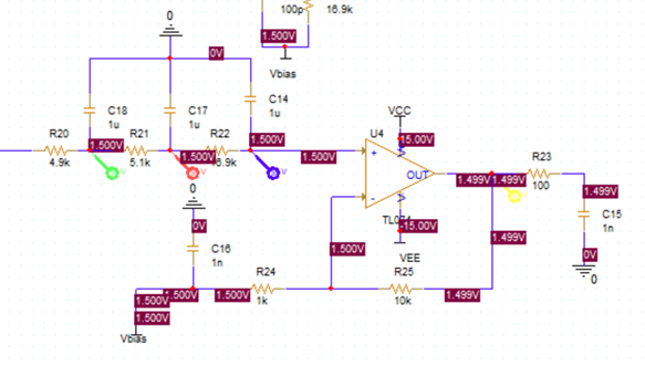
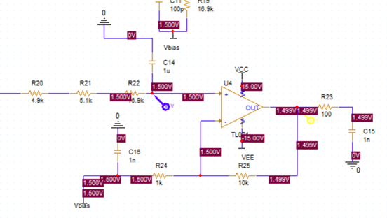
Good to see that in the new inverter project of my account, SiC FET is used to build the power stage, that means we can study the system effect of the SiC FET, but not only limited to the device itself.

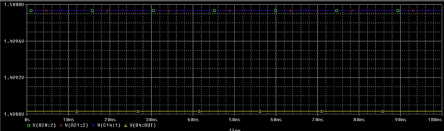
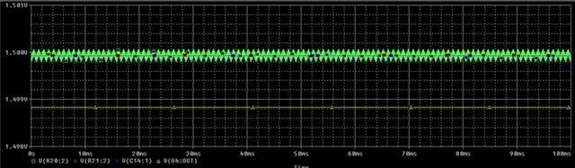
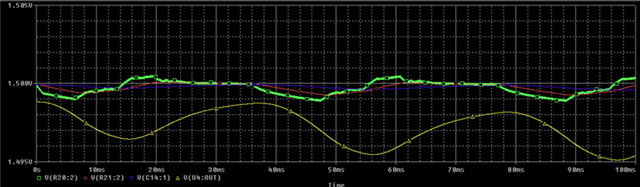
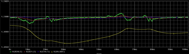
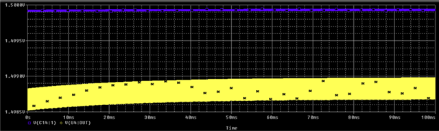
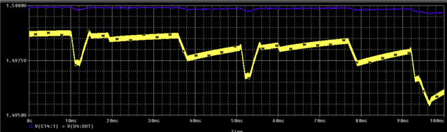
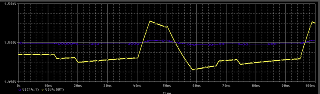
Now i meet the problem that when using SiC FET, the ultra short turn on and turn off time period causes a very high frequency noise which run through the PCB board and effect the input of TL074.

It causes a high common mode voltage between the positive input and negative input of the amplifier, and this should be suppressed through the circuit design.

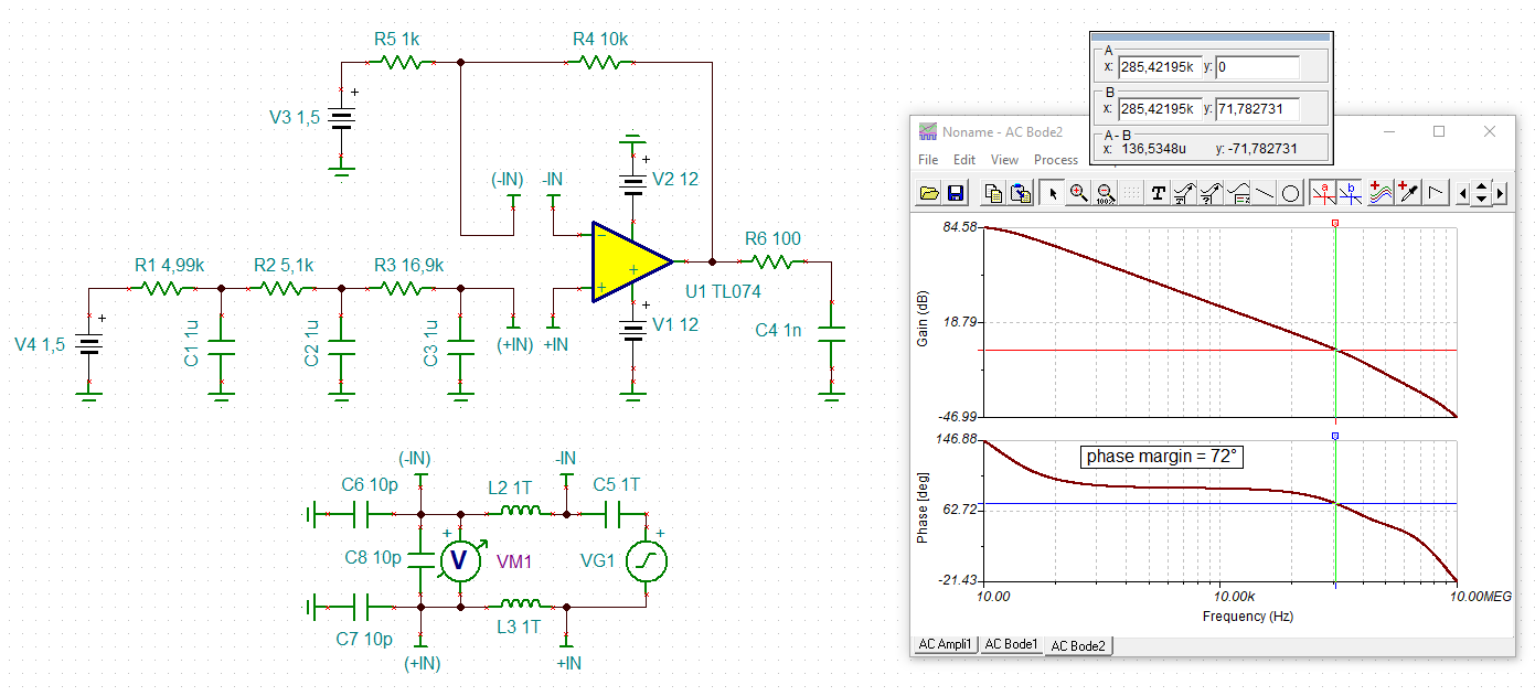
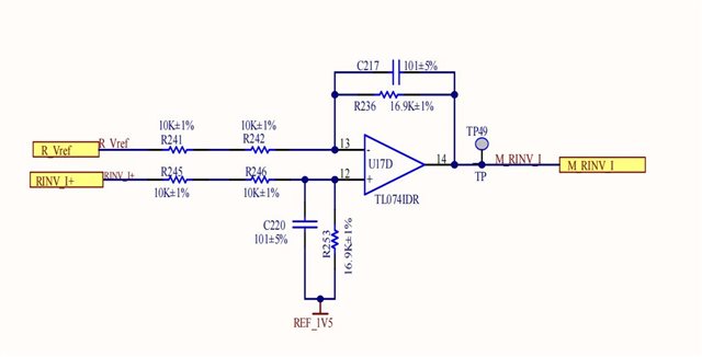
the question is: the traditional differential amplifier circuit needs a high resistance accuracy to suppress the common mode input voltage so it is not practical. is there any practical circuit design which do not need the high accuracy resistance at the same time has a high CMRR?

thank you

BR

  • Hi Br,

    do you have a schematic?

    Kai

  • Hi

    There still no progress on the schematic.

  • Hi Joe, 

    Along with the schematic, do you also have some information on what you are measuring on the input pins on the TL074? 

    Thanks!

    Best Regards,
    Ashley

  • Hi Ashley

    The problem is partially resolved after i debugged the circuit with customer. But there are still some questions make me confused.

    Let's see the original circuit, the input signal of TL074 is the output of the other TL074.

    The signal which connected to the  + input of TL074 is a 50Hz sine wave the average value of this signal is 1.5V the minimum value is close to 0V and the maximum value is close to 3V. The signal which connected to the – input of TL074 is a 1.5V DC reference. The triple RC circuits connected to the + input are designed for wave filtering, because this circuit is used in an inverter, there are some high frequency crosstalk generated by the power FET and may interfere the input signal.

    But after I added some different frequencies small signal interferer to the + input, the simulation results are very different, let’s see some pictures:

    This picture shows the different measurement points and corresponding color:

    +input: 1.5V dc signal:

    +input: 1.5V dc signal + 40kHz 0.1V sine wave:

    +input: 1.5V dc signal + 50kHz 0.1V sine wave:

    +input: 1.5V dc signal + 150kHz 0.1V sine wave:

    AS we can see in the picture, as the crosstalk frequency varies, the voltage of different measurement points also change, and the output error of TL074 become large.

    Then I changed the triple RC circuits to the single RC circuit as shown below

    The same crosstalk interferer are added:

    +input: 1.5V dc signal + 40kHz 0.1V sine wave:

    +input: 1.5V dc signal + 50kHz 0.1V sine wave:

    +input: 1.5V dc signal + 150kHz 0.1V sine wave:

    AS we can see in the picture, the output signal is different from the triple RC circuit. The interesting thing is that when the crosstalk frequency is 150kHz the output signal become better than before.

    Then I changed the customer‘s RC circuit form triple to single, the output error is improved a lot too, but I would like to discuss the reason why this change happen.

    Thank you

    BR

    Joe

  • Hi Joe,

    this can have to do with the filtering caps. Ceramic caps like Z5U are highly non-linear and the capacitance depends of the bias voltage. This can show very weird results. X7R is better but still problematic.

    I would check the circuit again with high quality plastic foil caps.

    Kai

  • Hi Kai

    Thank you for the discussion. 

    I find the C_load restriction of TL074 in datasheet 6.17, that the typical value of capacitive load drive is 300pF, but the original C parameter in customer's circuit is 3uF in total (see the wave filter circuit connected to "+" input of TL074, as mentioned before it is also connected to the output of another TL074). So I think if the exceeded C_load leads to the weird results.

    The simulation shows a good result after I adjust the capacitor to 0.3uF, and I verified the simulation result in customer's PCB.

    Maybe this question can be closed, and if there are still some questions in customer's further experiment I will discuss with you timely.

    Thank you so much!

    BR

    Joe

  • Hi Joe,

    I find the C_load restriction of TL074 in datasheet 6.17, that the typical value of capacitive load drive is 300pF, but the original C parameter in customer's circuit is 3uF in total (see the wave filter circuit connected to "+" input of TL074, as mentioned before it is also connected to the output of another TL074). So I think if the exceeded C_load leads to the weird results.

    The capacitive load specification of datasheet assumes a capacitance which is directly connected from the output of OPAmp to signal ground. But here a series resistance of 4k99 is mounted between the output of OPAmp and the three 1µF filter capacitors. This resistance very effectively isolates the output of OPAmp from the capacitive load. In this case the load capacitance can be heavily increased beyond 300pF.

    Kai

  • Hi Kai

    Yes, I have searched online the the series resistance can increase the load capacitance of amp, and tried one 1uF capacitor, the output of TL074 still stable. But three 1uF capacitors make the output unstable, so I would like to calculate how the phase margin improved by the series resistance, and verify through simulation and experiment.

    Joe

  • Hi Kai

    there is another new finding.

    the front stage TL074 is not in the same PCB with the rear stage TL074, so there is a long signal transmission line between two amplifier.

    I have done the experiment, that when the crosstalk occurs in the negative feedback loop of amplifier, it can be suppressed well and the output waveform is good, but when the crosstalk occurs on the transmission line out of the negative feedback loop, it seems the interferer can be out of controlled, and the output waveform becomes bad.

    But now, the long transmission line in customer's design is hard to be changed, is there some method to improve the circuit performance without changing the design too much?

    Thank you!

    Joe

  • Hi Joe,

    the front stage TL074 is not in the same PCB with the rear stage TL074, so there is a long signal transmission line between two amplifier.

    Please post a scheme showing how exactly the two TL074 are connected to each other.

    But three 1uF capacitors make the output unstable, so I would like to calculate how the phase margin improved by the series resistance, and verify through simulation and experiment.

    I would need to see the schematic of the driving TL074. So please post a full schematic.

    The phase margin of the receiving TL074 can be simulated as follows:

    joe_tl074.TSC

    But keep in mind that the Spice model of TL074 is very old (1989) and is highly simplified. It might not give proper results.

    Also, this transmission line stuff isn't included so far.

    Kai

  • Hi Kai

    Thank you for the simulation file, I also simulated that on Pspice, the result is the same as yours.

    The full schematic is shown below. The input of the first amp is a voltage signal from hall sensor. The first amp is located in the PCB board of three-phase AD/DC converter. The second amp is located in the PCB board of control MCU. The two PCBs is linked by dupont line.

    Thank you!

  • Hi Joe,

    I would insert an isolation resistor into the output line of first OPAmp. This will isolate the output from the capacitive load of flat ribbon cable and stabilize the OPAmp. Install a 220R resistor directly at the output pin of U17D.

    You can try to increase R342 from 100R to 220R as well.

    The TL074 is one of my favorite OPAmps. But because this OPAmp is so fast it doesn't like direct capacitive loads at the output very much. That's why I always install a sufficiently big isolation resistor.

    Kai

  • Thank you Kai, I will try it on customer's circuit, if there is any news I will reply you

    Joe

  • Hi Ashley

    I appreciate that the expert team strongly supports my work , there is no more question.

    Thank you

  • Good luck Relaxed

    Kai