This thread has been locked.

If you have a related question, please click the "Ask a related question" button in the top right corner. The newly created question will be automatically linked to this question.

THS4521 Single-Ended to Differential Converter

Other Parts Discussed in Thread: THS4521, TINA-TI

Hello!

I have an application which requires conversion from a single-ended input to a differential output for a high-precision ADC.  I only have access to a +5V source, so my initial design was as follows, mirroring the application note.
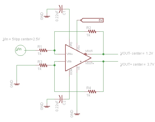
 

This yielded less than awesome results on the ADC, which took the off-center differential signal and turned it into a huge DC offset, thus getting rid of half my dynamic range.  Interestingly, though, when I do this (below), the problem goes away and the signal centers more or less properly:


Now, elementary circuit analysis tells me WHY this is.  Grounding the inverting input creates a voltage divider with R3 and R4, which is replicated for the inverted output by R1 and R2.  This is because I blindly assumed that the top circuit is how this SHOULD work.  My question is, what is the proper way to implement this?  Should I:

A) AC-couple the input, so that it floats around ground instead of 2.5V when going into the THS4521?

B) Tie the business end of R3 to either a 2.5V supply or a strong voltage divider, so that my differential in is compared to that instead of ground?

C) None of these

Any help would be greatly appreciated.

Phil

  • Hi Phil,

    The reason for the large differential DC offset (Vout+ = 3.75, Vout- = 1.25) is because there is effectively a differential input DC offset of 2.5V due to the inverting input to R3 being tied to ground.

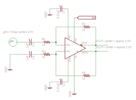
    Option A) will work if you AC couple the input signal into R1 and also add the same value of capacitor in series between R3 and ground. In doing this, the Vin+ and Vin- pins will float to the output common mode of 2.5V.

    Option B) will also work. By tying R3 to 2.5V instead of ground, the equivalent differential input signal will only consist of the 5Vpp signal and will not include the 2.5V DC bias of the input signal. See the attached TINA-TI simulation circuit for this configuration.

    THS4521 SE-Diff 6-14-2011.tsc
  • Hi Kristoffer,

    Thanks so much for your quick response.  I wired up Option A and it worked great, or so I thought at first.  The new circuit is as follows:

    This got rid of the offset issues (and even cleaned up some noise I was dealing with).  Now, the next problem.  The output of this circuit is going into a differential ADC.  Quite correctly, and just like in the TINA simulation, a 5Vpp signal on Vin yields two opposite 2.5Vpp signals on Vout+ and Vout-, whose difference is 5Vpp.

    I would like to add 2x gain in order to get the full scale of the ADC, so my first instinct was to change R2 and R4 to 2k resistors.  This succeeded in amplifying the signal, but also brought in very strange high-frequency noise/distortion on the negative side of the sine wave.  (In both the differential outputs and on the single-ended input).  I got the same results when I switched R1/3 to 500 ohms and R2/4 back to 1k.  I was unable to reproduce this in TINA.  And thoughts as to why this could be?

    The circuit pictured above works great, but only with R1=R2=R3=R4=1k.

    Thanks,

    -Phil

  • Phil,

    I do not see an apparent reason for this noise. Can you please post a screenshot that shows this noise?

    Would you be able to share the part number of the ADC you are using? What passive circuitry do you have between the THS4521 and the ADC inputs?

  • Kristoffer,

    Never mind, the issue ended up being in an earlier amplifier stage, or its interaction with the THS4521.  It's all fixed now, thanks so much for your help!

    -Phil