Because of the holidays, TI E2E™ design support forum responses will be delayed from Dec. 25 through Jan. 2. Thank you for your patience.

This thread has been locked.

If you have a related question, please click the "Ask a related question" button in the top right corner. The newly created question will be automatically linked to this question.

TIA for single-ended amplification of the differential mode signal of a BPD

Other Parts Discussed in Thread: LMH32404, ONET8551T, OPA855

Hi Team,

Do we have  device that meets the customer's specifications below?

I want a TIA that can perform single-ended amplification of the differential mode signal of a BPD, i.e. two identical PDs connected in series. The TIA can have more than one channel and support multiple BPD amplification. I would like the TIA to be a module with an RF interface (e.g. SMA, or BNC). Bandwidth does not need to be high, greater than 1GHz is sufficient. Also meet AC coupling.

Regards,

Danilo

  • Hi Danilo,

    a balanced photodetector (BPD) must have the connection point between the two photodetectors being connected to a DC virtual ground. Otherwise uneven illumination of the the both photodetectors will cause an imbalance between the photodetectors resulting in a ruin of indivual DC biasings. Because of this, AC coupling to the -input of TIA is no good idea.

    But you can bias the +input of TIA with an offset voltage (pseudo ground) -say middsupply-, of course, and DC couple the connection point of the balanced photodetectors to the -input of TIA which will see the mirrored pseudo ground potential of the +input of TIA (principle of virtual ground). To work properly, the biasing potentials of the both photodetectors would need to be modified then to correct for this offset voltage.

    Kai

  • Hi Kai,

    Thank you for your comments. Can you please suggest a device that would fit our customer's requirements?

    Can choose to match my current BPD TIA, which should be coherent communication field TIA, and then match my current 4 BPD 4-channel TIA, and then the rate does not need too high 5GHz down, AC coupling, want to achieve TIA and silicon optical chip of the common package, so the bare chip TIA. The size of bare die TIA needs to be small(width within 6mm).

    I understand that we don't have a bare die but could you please suggest a device in small package?

    Regards,

    Danilo

  • Hi Danilo,

    I have a few questions regarding the design parameters which will affect which TIA is best suited for their application. The questions I have are:

    What is the expected input capacitance of the BPD?

    What is there desired transimpedance gain? Also, the bandwidth they are trying to achieve.

    Is there a maximum package area (mm2) they are searching for?

    This information will be very useful in understanding which part best suits their needs.

    Best Regards,

    Ignacio

  • Hi Ignacio,

    Please see the response of our customer below.

    desired transimpedance gain> 5000V/A , larger is better ;
    the bandwidth > 1GHz
    maximum package area:no constraints, large size is allowed
    expected input capacitance of the BPD : the junction capacitance of PD is about 30fF

    Regards,

    Danilo

  • Hi Danilo,

    Can you clarify the 1 GHz bandwidth spec. Is that their intended operating frequency or the GBP they need from the device. Could you maybe give an expected range of rise times their application requires, this helps us narrow down their closed loop bandwidth requirement. However, I can offer a potential solution to your application. 

    The LMH32404 is a 4 channel TIA which integrates ambient light cancelation offering an alternative to ac coupling. It has a fixed gain of 20k V/A well above the 5k V/A requirement.  It is a slower part, which may result in a change to a different TIA, but this part does highlight some features you mentioned in a previous post.

    Best Regards,

    Ignacio

  • Hi Ignacio,

    Here is the response of our customer.

    1GHz for frequency
    I should make my requirements clear:
    1. I do not need integrated one, the one with RF ports(such as SMA or BNC) is needed
    2. size is not the factor to be considered
    3. four channels, two channels and one channel, all is ok, but we prefer more channels
    4. AC coupled is better , but without it is still ok.
    5. performance is which we care
    bandwidth(frequency) >= 1GHz
    transimpedance gain> 5000V/A , larger is better
    minimum NEP is expected to be around 10 pW/sqrt(Hz)---50 pW/sqrt(Hz), smaller than that is ok

    Regards,

    Danilo

  • Hi Danilo,

    After reviewing the customer's requirements, we do not currently have any TIAs in our op amp portfolio that can meet your 1 GHz requirement. There are parts such as the ONET8551T that are capable of these speeds but behave slightly differently than the traditional TIA. It does come in a bare die like the customer mentioned in a previous post but there are no evaluation modules with RF ports for this part since it is just a bare die.

    Best Regards,

    Ignacio

  • Hi Danilo,

    hhm, is the customer perhaps looking for a "RF gain block amplifier"?

    https://www.ti.com/rf-microwave/rf-amplifiers/rf-gain-block/products.html#p62max=1000;6000&p1241=RF%20Gain%20Block

    Kai

  • Hi Ignacio and Kai,

    According to our customer,

    The ONET8551T’s performance is good to satisfy my needs. But I still have one question.
    I need TIA for balanced photodetector. Ordinary PD may have GSG pad, and the bias voltage between S pad and G pad(no matter what G pad) is same. But for BPD which also has GSG pad, the bias voltage between S pad and different G pad is different, that means these two G pads is different.
    Now ONET8551T can offer bias, and is that kind of bias can be applied to BPD? If it can’t , can you offer me a TIA that can offer bias to BPD. Thanks.

    For BPD, the signal we need is the AC current, so DC is need to be blocked. This is another big problem for me. I wonder if there exist a kind of TIA satisfy this demand.

    Regards,

    Danilo

  • Hi Danilo,

    as I already meanioned you should DC couple the connection point of a balanced photodetector (BPD) to the -input of TIA. Otherwise even the least imbalance between the two photodetectors may result in an imbalanced biasing.

    An example: Assume the one photodetector of BPD is biased by +5V and the other photodetector is biases by -5V with the connection point of the two photodetectors being AC coupled to the -input of a TIA. Then the least imbalance between the two photodetectors (dark current, ambient light, etc.) can result in a shift of the potential of connection point of BPD. Because of that, after some time the one photodetector may see a bias voltage of 0V and the other photodetector -10V.

    Only when the midpoint of BPD is DC coupled to the -input of TIA which forces the midpoint of BPD to ground potential such an imbalanced biasing can be prevented. An AC coupled TIA cannot do this.

    Kai

  • Hi Kai,

    Please see the feedback of our customer.

    Thank you for your reply. And I still have some questions about your reply and the TIA.

    For the BPD, there are two current loops at the same time, the RF loop and the DC loop.

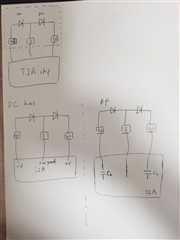
    Question 1 : The DC loop involves the biasing of the BPD. Can the TIA provided by Texas Instruments provide a +V bias to the G1 pad and a -V bias to the G2 pad, as drawn in my diagram, so that each PD is in reverse bias and has the same bias voltage?

    Question 2: Since the implementation of AC coupling at the RF signal output (S pad) is problematic. Then is a capacitor connected to the G pad provided inside the TIA to isolate the possible common mode DC noise in the RF loop? This is necessary for BPD, so is there a TIA that provides such a feature (capacitors inside TIA to block DC noise in the RF loop)?

    Regards,

    Danilo

  • Hi Danilo,

    Question 1 : The DC loop involves the biasing of the BPD. Can the TIA provided by Texas Instruments provide a +V bias to the G1 pad and a -V bias to the G2 pad, as drawn in my diagram, so that each PD is in reverse bias and has the same bias voltage?

    I do not see a diagram.

    Kai

  • Hi Kai,

    I apologize that I forgot to upload the diagram. Please see the file below.

    Regards,

    Danilo

  • Hi Danilo,

    I will take this information and get back to you with a response. Thank you for your patience.

    Best Regards,

    Ignacio

  • Hi Danilo,

    I'm sorry, but I don't understand the diagram. What terminals shall be DC biased to provide a reverse voltage to the photodetectors and what terminal(s) shall be connected to the input of the TIA? Or do you need two TIAs in the end, one for each photodetector?

    Kai

  • Hi Kai,

    Please see the feedback of our customer.

    Take ONET8551T for example, The datasheet shows a way to connect between the PD and ONET8551T. Now we change ONET8551T's connection to a BPD (a cascade combination of two PDs, again with three GSG pads connected to the chip). For the PD, the bias provided by ONET8551T is G1 = G2 = +V, S = 0V (as an example, not necessarily accurate), which is the same bias voltage that ONET8551T added to the two G pads. But for the BPD, it needs G1=+V, G2=-V, S=0V, which is the bias voltage needed on the two G pads is different. For ONET8551T , can it provides that kind of bias voltage(G1=+V , G2=-V, S=0V)? Or is there a kind of TIA chip provided by Texas Instruments can satisfied that needs?

    Regards,

    Danilo

  • Hi Danilo,

    After looking into the applicability of a BPD and our ONET devices, the set up the customer needs will not work for these devices. These devices have large bandwidths, DC input current cancellation, and respective pads to bias the photodiode but the ONET devices are configured and designed for a single photodiode.

    Since an ONET device is not ideal in this application, a possible solution is to implement a multi-stage solution which can be designed to remove the DC component of the signal after the TIA. Kai highlighted this solution very well in this thread. Our fastest TIA is currently the OPA855, which by scaling down the gain might be able to get the bandwidth they are looking for. This multi-stage set up might be a suitable option for the customer as we do not currently have devices in our portfolio that are capable of these performance requirements.

    Best Regards,

    Ignacio