This thread has been locked.

If you have a related question, please click the "Ask a related question" button in the top right corner. The newly created question will be automatically linked to this question.

INA337: Amplifying Load Cell Signal

Part Number: INA337
Other Parts Discussed in Thread: INA326,

Hi,

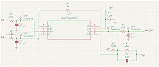
I am amplifying a tension and compression strain gauge type load cell with the INA 337, but I am running into issues.

Two issues I am having.

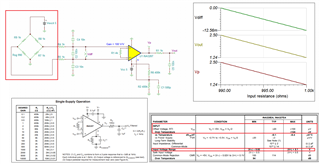
1. I am unable to provide the load cell signals to the amplifier unless I have a buffer on each input. However I feel like this should not be the case as there should be already a very high input impedance on the amplifier

2. The amplifier does not work when I do an offset voltage. So I am trying to offset my output by 2 volts (hence the 4v at pin 5) but whenever I use this circuit my load cell input is not amplified and the output of the amplifier is stuck around 2.3 volts

Also when I measured current between the load cell signal and the amp input there was a current of 9mA coming from the amp to the load cell.

Am I doing something wrong in my circuit?

Thanks,

Allen

  • Hi Allen,

    The load cell input signal is are required to establish a proper common mode voltage, say 2.5Vdc. We do not have Tina simulation for INA337, but INA326 is the closest one to the instrumentation amplifier. The INA337 is a wide-temperature (-40C to +125C) version of the INA326, with some minor electrical differences.

    Enclosed is a simulation of INA326 with parameters that resemble to yours. 

    INA326 Load CellA 11012022.TSC

    Regarding to establish the proper input Vcm voltage, here is Vcm vs. Vout linear relationship. If you are interested, you may download it from the link below. 

    https://www.ti.com/tool/ANALOG-ENGINEER-CALC

    FYI, here is a copy of input differential and common mode filtering configuration and equations. 

    https://www.ti.com/lit/ug/sbou115c/sbou115c.pdf?ts=1667338864690&ref_url=https%253A%252F%252Fwww.google.com%252F

    If you have additional questions, please let us know. 

    Best,

    Raymond

  • Thanks for the quick reply Raymond

    I'm not sure if I completely understand your response? Is there something wrong with my schematic that would cause my amplification to not work? I believe that I followed it correctly but am not able to get the behavior I want.

    The only difference between my circuit I built and the images of the model you sent over is this capacitor C2. What does this capacitor do and is it necessary for proper function?

    Thanks,

    Allen

  • Hi Allen,

    The only difference between my circuit I built and the images of the model you sent over is this capacitor C2.

    From the initial schematic, it is not clear what is your common mode input voltage is. I suspected that there is no or not large enough common mode voltage, Vcm due to single supply rail IA configuration. 

    Without proper Vcm, The Vcm vs. Vout will look like the following, where the input and Vout will not operate linearly. 

    The input will have to establish a proper Vcm input voltage, shown in green line in the diagram below. With the proper established Vcm, say middle rail of your load cell excitation voltage, the differential input signal is riding on top of Vcm. 

    Note: if the IA is configured with dual supply rails, then Vcm can be near ground and the IA will operate linearly. Since the circuit is using 5Vdc single supply, you need to have a proper Vcm voltage. 

    In terms of C2, this is to provide the input front with the differential input LPF. The initial circuit implemented the common mode LPF and the differential input filter needs to be placed in front to the common-mode filter. The input analog front only amplifies the differential input signals, and remove the common mode noise or voltage, like Vcm. 

    I have enclosed all necessary tools for you to simulate the IA. If you have additional questions, please let me know. 

    Best,

    Raymond