This thread has been locked.

If you have a related question, please click the "Ask a related question" button in the top right corner. The newly created question will be automatically linked to this question.

INA828: How to design the input filtering circuit for the IC INA828ID (common mode filter and differential mode filter) and Phase shift of the circuit attached?

Part Number: INA828
Other Parts Discussed in Thread: TINA-TI, , INA326

Hi,

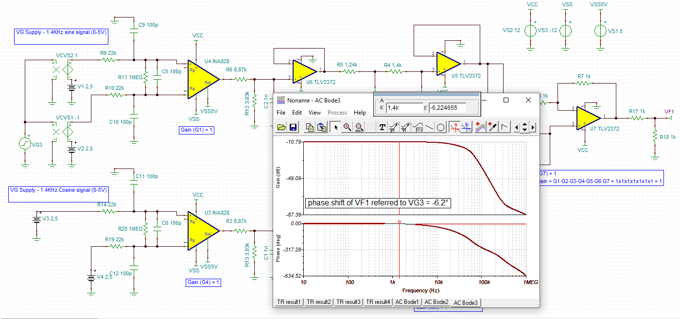
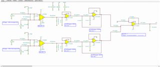
  • The below attached circuit converts the differential sine and cosine signals to single ended signal, it is then filtered using a 3rd order low pass filter, finally the filtered cos and sine signals are summed and sent to the ADC of TMS320F28377DPTPEP (ADC voltage range is 0V to 3V) controller.
  • How to design the input filtering circuit for the IC INA828ID (common mode filter and differential mode filter)?
  • Considering the circuit attached below how to theoretically calculate the phase shift of the circuit (Phase shift calculated between the input (COS+SINE) and output (COS+SINE))?
  •  Input to the circuit (INA828ID) is differential sine and cosine signals of 1.4k Hz (0V - 5V).
  • The 3rd order LPF circuit has cutoff frequency of 60K Hz.

SINE COS.TSC

Thank you.

  • Hi Mahima,

    you can do a theoretical calculation of phase shift by considering the phase shifts of all involved low pass filtering circuits or you can simply do it by the help of TINA-TI simulation:

    mahima_ina828.TSC

    Or like this:

    Kai

  • Hi Mahima,

    referring to the common mode and differential input filtering there's no simple answer. It depends on how much EMI and noise needs to be filtered out. Resistors at the inputs add noise and cause additional input offset voltage caused by the input offset current. So for highest precision and lowest noise the input resistors should be kept <1k. But if the increase of noise and input offset voltage doesn't play a role in your application because your signals are big, then you can increase the input resistors somewhat (1k...10k).

    For proper differential filtering the filter resistors should at least be 20 times higher than the source resistances. Otherwise unwanted shifts of corner frequency and phase shifts of wanted signal can occur. The filtering cap and by this the corner frequency of differential low pass filtering should then be chosen to cause no unwanted signal dampening or phase shift.

    For proper common mode filtering the restrictions are way higher. For optimum common mode rejection the filter resistances should be at least 100 times higher than the maximum imbalance of source resistances. The imbalance of source resitances is one major source of unexpected decrease of common mode rejection when using an instrumentation amplifier. The two filtering caps of common mode low pass filtering should be chosen very carefully, because even the least imbalance can totally ruin the common mode rejection of instrumentation amplifier. In any case very low toleranced caps with very low temp coefficients and very low long term drifts should be chosen. 1% toleranced ceramic NP0 or COG caps are a good choice. But even then you may see a massive degradation of common mode rejection caused by additional imbalance introduced by uneven stray capacitances. Because of this the filter capacitances should be way higher than the expected stray capacitances. Another remedy to enhance the common mode rejection is to choose a very high corner frequency of common mode low pass filtering and to keep the corner frequency far away from the frequency of wanted signal.

    Keep in mind:

    1. Signal filtering is done by the differential filtering, EMI filtering by the common mode filtering.

    2. Common mode filtering can do more harm than good. "Less is more."

    Kai

  • Hi Mahima,

    Kai has covered the INA828 CM/DM input filter topic very thoroughly. The only thing I might add at this point is you may wish to consider using an X2Y capacitor structure, in place of the 3 separate input filter capacitors. The X2Y capacitor's design and physical structure provides inherently good matching between the 2 CM capacitors, the 2 "Y" portions of the X2Y capacitor. This affords more precise matching of the two DM input filter paths. The X2Y is available using the high performance C0G dielectric that Kai mentions. The "X" potion of the capacitor is the DM X2Y capacitance.

    I show below an image of an X2Y capacitor used in a INA326 input filter. The X2Y has lower self-inductance (ESL) than some MLC capacitors and that means they come closer to providing a more ideal capacitor function in the filter. Additionally, due to their low ESL the X2Y make very good power supply bypass capacitors also seen in the image.

    Several different capacitor manufacturers are licensed to produce the X2Y capacitor. I used the insertion loss information that Johanson published for their X2Y product.

    Regards, Thomas

    Precision Amplifiers Applications Engineering

  • Hi Kai,

    Thank you so much, this resolves my issue.

  • Hi Thomas,

    Thank you so much, this resolves my issue.