This thread has been locked.

If you have a related question, please click the "Ask a related question" button in the top right corner. The newly created question will be automatically linked to this question.

THS7530-Q1: Noise problem

Part Number: THS7530-Q1
Other Parts Discussed in Thread: THS7530, THS4541

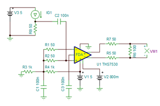
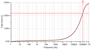
We're using the THS7530 VGA chip on one of our new projects, and we're having a noise problem. According to the specification of THS7530, the noise of the chip is 1.1nV/Hz. In contrast, the noise of the high-speed operational amplifier THS4541 is 2.2nV/Hz. I try to use TINA simulation software to build a simulation circuit for the noise test of the two chips. The test results show that the total noise output of THS7530 and THS4541 at 200MHz is about 200uV and 70uV respectively. The simulation circuit and data are shown in the figure below.
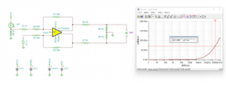
However, after the actual production of these two circuits, we used oscilloscope to test the noise of these two circuits, and the noise of THS7530 is about 2.6mV (RMS), which is more than 10 times larger than the simulation data, while the noise of THS4541 is 0.13mV, which is similar to the simulation data. We have made a total of 5 test boards of THS7530, and the noise results are all 2.6mV, which can exclude the possibility of single chip abnormality. In addition, we also purchased the demo board of THS7530 by TI, and the noise tested was also about 2.6mV.

Your help and assistance are urgently needed.

thank you

  • Hi,

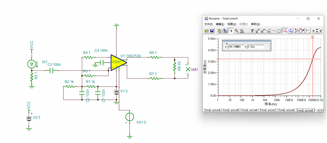
    I think the problem is that you have grounded the Vocm pin, therefore it is out of range:

    I've repeated your simulation and used midsupply Vocm as the datasheet recommends:

    and I got this total noise:

    It seems to fit your experimantal results.

    Do not forget: the 1.1nV/√Hz it the input noise, here you have a gain of about 100 for the amplifier.

    Best wishes, Zoltan

  • in my test circuit board ,Vocm is floated with 100nF cap and set the gain as minimum but the noise is still about 2.6mV. Is it normal? 

  • in my test circuit board ,Vocm is floated with 100nF cap and set the gain as minimum but the noise is still about 2.6mV. Is it normal? 

  • Hi,
    I think it is normal. A TI expert could tell you more, but I think, that this chip can be considered as a fixed gain amplifier with an analog multiplier (Gilbert-cell is shown in the datasheet) at its input. So, the voltage noise gain is practically fixed, independent of the gain control voltage.
    Zoltan

  • Thanks for you reply, that's realy help. But I'm still confusing why the noise is so large. You mean the main noise is contributed by the Gilbert-cell architecture?Are there any high speed VGAs as the same as OP-AMP with lower noise?

    And in THS730's datasheet, the noise figure is worse, but total input voltage noise looks OK, what dose the total input voltage noise mean? Feel no reference significance, but easy to be misunderstood by this parameter.

  • Hi,

    The noise is not large at all, in fact, it is very low! What do you expect, if you have gain of 100 and bandwidth over 200MHz? 

    At the output your see hundred times the amplifier’s input noise density integrated over the bandwidth. Do a simple calculation:

    1. amplifier noise at the output = 100 *  square root ((1.1nV)^2/Hz*200MHz ) 1.56mV

    2. the R=100Ohm equivalent resistance (sum of your R3 and R4 resistors) at the input generates thermal noise at the output = 100 * square root(4*k*T*R*200MHz) 1.82mV, larger than the noise of the amplifier!

    3. their combined noise at the output is square root of (1.56^2+1.82^2) mV ≈ 2.39mV, that fits your observations quite well.

    You operate the THS4541 at unity gain, of course you have much smaller output noise.

    Use TI training materials to learn more about how to deal with noise: Calculating RMS noise and Calculating total noise related to your problem closely.

    Zoltan

  • Hi Zoltan,

    Something feels wrong. In fact, when I tested, the gain was not set to such a large size. I set the gain setting voltage to 0V, about 2-3 times, and the noise output of the test was also about 2.6mV, which did not change with the adjustment of the gain. I also tried to set the input resistance to 1Ω in the simulation circuit, which produced even more noise. Read other people's answers to questions, it was mentioned that VGA design is constant noise output. I wonder if the noise caused by the Gilbert-cell architecture is too large or what other causes the noise to be more than 10 times larger than the operational amplifier.

  • refer to e2e.ti.com/.../ths7530-about-noise-figure

    many of the todays VGAs use a topology which provides a constant output noise. But this means, that the input reffered noise depends on the set gain. The higher the set gain, the lower the input referred noise. This is what figure 3 of datasheet shows.

  • Hi,

    Think about this device as a voltage-controlled attenuator followed by a fixed gain amplifier. Lower signal gain is achieved by attenuation of the input signal before applying a large fixed gain. Therefore, you always have the same internal gain and noise at the output, you can only change the input signal attenuation.

    In your last simulation you’ve changed the output voltage divider (R6, R7, R8), therefore you’ve practically doubled the output voltage and consequently the overall gain. So the 1 Ohm resistors at the input did produce smaller noise, as expected.

    In conclusion neither the Gilbert cell nor the amplifier generates large noise. The difference between the signal gain and internal fixed gain is what can make you confused, but I hope now it is clear enough. Every architecture has its advantages and disadvantages. It depends on the application, if you really need the features what this amplifier offers.

    Zoltan

  • Ok, is it sure that the noise level of THS7530 chip is the one I tested, about 2.6mV, not caused by my testing error?

    In addition, our requirement is that the gain of 2~4 times can be adjusted through the function of VGA chip, but the noise should be less than 1mV. Is there any other more suitable scheme to achieve this? And the scheme should meet the AEC-Q100 certification.

  • Hi,

    As you see, your results are in agreement with the simulations, other posts and noise calculations.

    If you need gain between 2 and 4 only, you can choose another solution that fits better. To do so, I think you should consider the following:

    • Do you need continuous gain control or is it enough to switch between gain of 2 and 4? How many gain steps are required?
    • If you process your signal using an ADC, the gain range of 2 to 4 means only one more bit of resolution. Is it really needed?
    • What is the required bandwidth? The higher the bandwidth the more noise you get.
    • How accurate the gain should be?

    There can be several other points of course, but these can be used to choose the amplifier architecture.

    Try to find out your needs as carefully as you can and then use the parametric search on the TI website. There are voltage controlled amplifiers, variable gain amplifiers, programmable gain amplifiers with various gain ranges and bandwidths. You can also employ multiple opamps with disable feature to implement switchable gain, see the Wired OR MUX and PGA Reference Design,

    If you need more help, I recommend you to start a new thread and ask your question as a new one. I think this thread should be closed.

    Good luck!

    Zoltan