This thread has been locked.

If you have a related question, please click the "Ask a related question" button in the top right corner. The newly created question will be automatically linked to this question.

ALM2403-Q1: the difference of PMOS drawing between datasheet and App note

Part Number: ALM2403-Q1
Other Parts Discussed in Thread: ALM2402F-Q1

Hi Team,

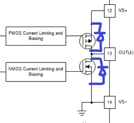
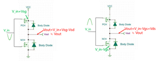
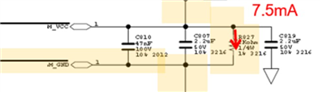
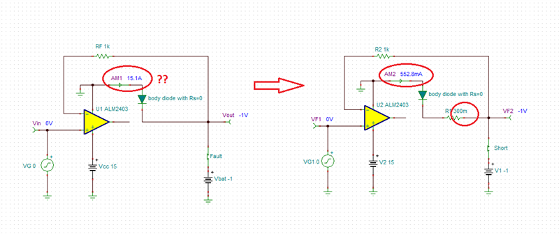
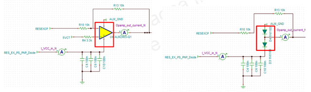
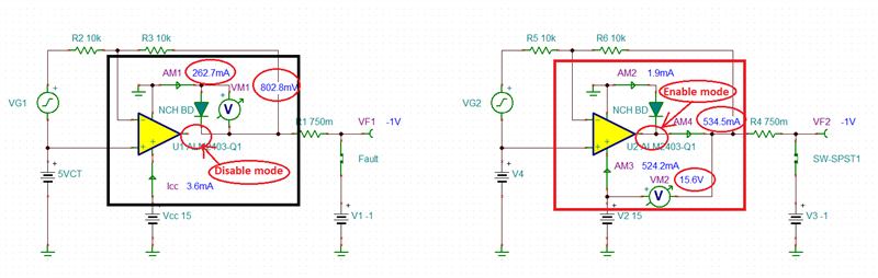
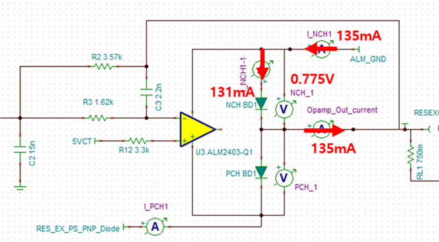
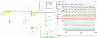
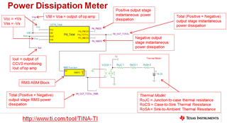
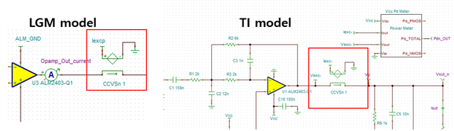
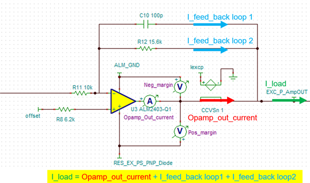
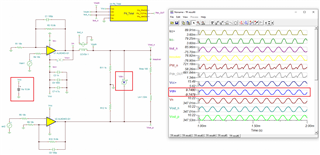
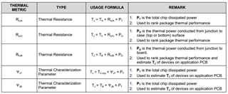
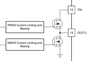
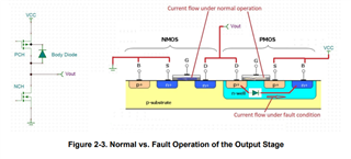
In the datasheet of ALM2403-Q1, the PMOS's  drain is connected to VS+. but the PMOS's  drain is connected to Vout at the App note as below. 

I think that PMOS's source pin should be connected to VS+. 

Please clear explain PMOS direction and body diode as well.

Best regards

Joey Kim

  • Hi Joey,

    Yes, your comment is correct.  The PMOS/NMOS drawing in the block diagram are incorrect.  We are in the process of revising the ALM2403 data sheet and hope to have it out by end of January, this will be one of the changes.

    The correct drawing should have the source connected to VS+ for the PMOS, and VS- for the NMOS.  The body diode polarity is shown below.

    Best Regards,
    Mike

  • Hi Mike,

    Thank you for your kind reply.

    if there is any other change items, please share it with me.

    also, please feedback below understanding is correct.

    Best regards

    Joey Kim

  • Hi Joey,

    There are many changes.  I can write you directly to get this information to you if you need it soon. 

    The schematic above is for a digital gate using CMOS; an amplifier will have a much more detailed circuit to drive the gates to create a Class AB biasing scheme.  We typically show our block diagrams with blocks for these stages:

    The block listed "Class AB Control Circuitry" is typically consist of additional current sources and MOS device.  I'm unable to find any further information in our collateral, but you can search "Monticelli Output Stage" for many examples of a commonly used output stage architecture. 

    Hope this helps,
    Mike

  • Hi Mike,

    Please send the information thru the email.

    LG Magna will fix the solution by next week and need to know more information.

    also, please check the below calculation and give a feedback.

    there are some test condition ( Vout is -1V ) in the disable ( SH_DN = Low), and below is that LG Magna calculation.

    if it is not real calculation, please share the our calculation or simulation model for disable case.

    And Vf value of Body diode as well.

    Power1 = Vf *If = 0.7V*0.22A
    Power_total = Power1 + Power2
    TJ= Power_total *Rth_J_A(46.9C/W)+T_A 

    Best regards

    Joey Kim

  • Hi Joey, 

    What is the ALM2403-Q1 driving application? 

    I believed that ALM2403-Q1 is driving a resolver load. If the following image is the load, then ALM2403-Q1 is capable to drive the load, shown in the image below (except for these paralleled capacitors). And it does not require the additional voltage source on top of the load. ALM2403-Q1 is an integrated resolver driver and it has all the required elements to drive the resolver application. 

    I sent you a message via our internal email. If you want to discuss the application, please provide us the design requirements and load parameters. This is a public E2E forum, and we can support in either forums. Please let us know. 

    Best,

    Raymond  

  • Joey,

    In a disable mode with Vout shorted to 1V below the negative supply, ALM2403 body diode current will be a function of the diode saturation current (Is) and series resistance (Rs). Assuming Rs of zero ohms this could result in a very high current, which could damage body diode - see below on the left.  For this reason to be on the safe side, I would recommend adding a small R1 300mohm (1W) output resistor to keep the current below 1A (see below on the right) unless something else already limits the current to 220mA as shown in your customer's calculations  - I am not sure where 220mA comes from.

  • Hi Marek,

    Below is LG Magna additional question.

    1. Please see the attached figure with 220mA current flow. Additionally, we added 0.75ohm at the output of opamp to limit the current. Is the only safe requirement for body diode that current flow should be smaller than 1A ? Otherwise, is there any requirement of power or other limitation?
    2. Could you give us guidance to calculate power consumption at shut down.

    3. Also, It is feasible to simulate fault conditions with 2 diodes like below figure ?
    For body diode model, could you share the body diode model for the simulation ? If it is not impossible, could you reply which diode model in the TINA catalog Editor can be used for the simulation ?

    Best Regard

    Joey Kim

  • Joey,

    The figure you attached does not show the 220mA current path so I'm still not sure what limits the current to said value.

    1. If the current through the body diode is limited to 1A, it will result in a certain forward bias voltage across the diode and thus limit the power dissipation inside the package to P=AM1*VM1 - see below.  Since the power dissipation across the series output resistor is outside the package, this does NOT increase the Tj of ALM2403-Q1.

    2. ALM2403-Q1 in a shutdown mode with 750mohm series output resistor will greatly limit the current - see below on the left. We did not characterized the NCH body diode BUT using my engineering judgement the AM1 current could be in the range of 262mA resulting in total power dissipation inside ALM2403-Q1:

    P_total_Disable =  0.263A*0.802V + 0.0036A*15V = 0.262 Watt

    The same ALM2403-Q1 in an active mode would result in MUCH higher power dissipation (see above on the right):

    P_total_Enable =  0.5345A*15.6V + 0.0019A*0.6V = 8.34 Watt !

    3.  Below I have attached my "engineering judgement" model, which should be close for the application here.  Since it is NOT based on the taken characterization data, the actual performance may be somewhat different but sufficiently close to determine power dissipation and resulting increase in the junction temperature, Tj.

    LG Magna ALM2403 Fault.TSC

  • Hi Marek,

    Thank you for your support.

    Is it okay to simulate fault conditions with below figure(Both NCH, PCH diodes are included)?

    The total input current(135mA) is larger(135mA) than the body diode current.
    The difference of 4mA seems to flow into power op amp.
    If it is the case, is the power consumption and junction temperature calculated as below?
    Ploss(0.105W) = total input current(135mA) *V_F(0.775V)
    Tj = Ploss(0.105W)*Rth_J_A(46.9C/W)+T_A(90) = 94.9C

    Best regards

    Joey Kim

  • Hello Joey, 

    Marek is out today and will he will be able to respond within the next business day. Thank you for your patience. 

    Best Regards,

    Chris Featherstone

  • Hi Marek,

    Please give a feedback.

    Best regards

    Joey Kim

  • Joey,

    It is not possible for 4mA current to flow into negative supply - all current on the negative pin must flow thru N-channel body diode. Having said that, assuming Ta of 90 degrees, your overall calculation of Tj is more less correct. 

  • Hi Marek,

    Please feedback.

    "if then, could I revise the calculation as below for correct calculation of Tj?
    Assumption : all current flows through Nch-body diode.
    Ploss(0.105W) = total input current(135mA) *V_F(0.775V)
    Tj = Ploss(0.105W)*Rth_J_A(46.9C/W)+T_A(90) = 94.9C"

    Best regards

    Joey Kim

  • Hi Joey, 

    The total dissipation calculation is correct, however, I would use the thermal resistance in Psi_JB figure, which is approx. 22.5C/W. The majority of heat from ALM2403-Q1 is dissipated via the thermal pad and PCB, and it would make more sense to use the thermal reference. 

    In addition, the junction temperature estimation in ALM2403-Q1 should be estimated from the total power dissipation in ALM2403-Q1, which is based on the average AC power dissipation across both Pmos + Nmos and power loss from Vsupply* Iq of the driver. From the total power dissipated at the ALM24-3-Q1, then you may be able to estimate the Tj at Tamb = 90C. (the application's worst case)

    If you are able to provide us all the related design requirements and load conditions, we are able to simulate the power dissipation in ALM2403-Q1 via Tina Simulation. 

    Best,

    Raymond 

  • Hi Raymond,

    Additional question of ALM2403 max output voltage

    : Thanks for quick response. From datasheet, the figure 6-13,14,15,16 shows the larger voltage drops from rails, considering our worst load current(180mA), compared to AoI gain(voltage drop:1.5V, RL:224ohm). Therefore we will have to refer to the figures.
    (1) Is it correct that Vs = +- 6V meens positive rail =6V and negative rail =-6V ?
    (2) We would like to know the max. output voltage @ 180mA, Positive rail = 13V and Negative rail = 0V. Is it okay to refer to figure 6-13and 6-14 for our condition? This is because not much big difference is shown with the different rail voltages.
    (2) We understand that TI is only able to give the typical value at certain load current.
    It would be great if TI could provide some safe margin value to rail voltages because the figures show only typical values and it could be over the linear operation range. For example, if the voltage drop @ certain current value is 2.7V with reference to fig 6-13, how much voltage margin is required, considering ALM2403 parameter change ? (e.g. 1V margin )

  • Hi Joey, 

    We have ALM2402F-Q1 and ALM2403-Q1 resolver drivers, and each driver has its Pros and Cons when operating over a wide temperature range. 

    Enclosed is the ALM2403-Q1 simulation that is prescribed in the application note below. 

    In the simulation below, resolver driving amplitude of 20Vpp is simulated, and power dissipation at ALM2403-Q1 is calculated. We are able to answer all of your inquiries, if you can provide us the resolver's load parameters and its configuration.  

    ALM2403-Q1 PWM + 3rd order LPF Driver 02162023A.TSC

    https://www.ti.com/lit/an/sboa504/sboa504.pdf?ts=1676578334996&ref_url=https%253A%252F%252Fwww.ti.com%252Fproduct%252FALM2403-Q1

    I am in the process of revising the ALM2403-Q1's datasheet. I sent you an email about a month ago. If you are able to reply me back via our internal email, I am able to send a copy of the revision draft in mean time.

    You mentioned that the calculated peak current may be up to ±180 mApk or ±180 mAavg. First of all, I would like to check the load current via the simulation. Also, we may be able to perform power factor correction from the load, and see if we are able to reduce the AC peak or average current and reduce the heat dissipation in ALM2403-Q1 driver. 

    Power factor correction equation is shown below (types of powers are Real power, Reactive power and Apparent Power; and we may need to reduce the reactive power and make the resolver behaves more like "resistive load". ):

    If you have additional questions, please let us know. 

    Best,

    Raymond

  • Hi Raymond,

    Thank you for you help.

    Below is LG Magna questions

    In the simulation below, resolver driving amplitude of 20Vpp is simulated, and power dissipation at ALM2403-Q1 is calculated. We are able to answer all of your inquiries, if you can provide us the resolver's load parameters and its configuration.
    ==>

    LGM


    1. : We only have resolve resistance, 100ohm +-14%. We do not have resolver inductance, now. The excitation voltage frequency is 10KHz. Do you think we can simulate the junction temperature of ALM2403 with only appling resolver resistance(with resolver inductance = 0)?? Does the reactive power affect the power comsumption of ALM2403?

    2. could you share the power calculation equation? Is it the same with below equation from the datasheet?

    3. From our simulation result, Tj (@Tambient:90C)is estimated as below, w/ Resolver resistance : 100ohm and inductance L0=:0mH.
    Is it correct to calculate the junction temperature with average power rather than max. power value which happens for a just brief moment? Could you guide us the parameter values for junction temperature estimation.
    Parameter values of a below list are required to be determined.
    (1) Rth junction to ambient : 46.9C/W or not ?
    (2) Power value : either max.(peak) power or average power from simulation result
    (3) Ambient condition : 90C is required for our worst condition.
    (4) EXC_P voltage and EXC_N voltage are generated by both Opamps in a package, respectively. Therefore power values of both ones are summed to calculate junction temperature. (the circuit design is different from TI application note design. we cannot share our design.)

    Best regards

    Joey Kim

  • Hi Joey,

    Does the reactive power affect the power comsumption of ALM2403?

    Yes, the reactive power can affect the total power consumption by up to 50% or so. n inductor, the voltage leads current by 90 degrees. Assume a resolver has input impedance in 100 + j188 Ω @10kHz, where ESL = 100Ω and inductance is approx. L= 188/(2*pi*f_10kHz) = 3 mH. The voltage leads inductive current per the resolver example is approx. θ = atan(188/100) = 62 degrees. In other words, the voltage and current are not in phase with each other. 

    In the case of 100 Ω resistor, voltage and phase are in phase with each other (the power applied to pure resistor refers to Real Power, power applied to inductor or capacitor refers to Reactive Power). The image below is the 3 power relationships. 

    2. could you share the power calculation equation? Is it the same with below equation from the datasheet?

    The power calculation equation is correct for resistive load, see the math derivation below. 

    Is it correct to calculate the junction temperature with average power rather than max. power value which happens for a just brief moment?

    The resolver transformer's winding resistance is 100Ω ± 14% and the primary and secondary resolver transformer's inductance will not be 0mH or this will not be elements in a transformer or magnetic coupling. 

    Is it correct to calculate the junction temperature with average power rather than max. power value which happens for a just brief moment?

    In AC power, it is referring to the average power (there is no maximum power as expressed in DC). If one has to express the max. AC power, you may say that it is peak AC power. Power is integral of V(t)*I(t) over time (in this case, the integral is from 0 to 100usec to derive the average AC power), see the slide above. This is an integration of AC power sinusoidal curve, thus it is the average power that will be applied and dissipated across ALM2403-Q1 drivers.  

    (1) Rth junction to ambient : 46.9C/W or not ?

    I would use the thermal resistance figured marked in green. Since the thermal pad will be soldered onto a PCB and this is the dominated heat dissipation method in the design, then the Tj should be used estimated from the ALM2403-Q1's heat dissipation. 

    (2) Power value : either max.(peak) power or average power from simulation result

    The average power dissipated across ALM2403-Q1's driver can be derived from the Tina Simulation. 

    (4) EXC_P voltage and EXC_N voltage are generated by both Opamps in a package, respectively.

    Yes, the sum of the dissipated average  power is the total average power dissipated  in ALM2403-Q1.Please see the example below. 

    Here is how to extract the power information from the plot. Once the signal is generated, you select the Total Power Curve from the simulation plot --> click on Process --> Average --> Average Value of the Power Curve. 

    Here is the power dissipation function inside of the previous simulation. 

    Once you obtained the total average power dissipated across ALM2403-Q1's drivers, you can back calculate Tj temperature at 90C, which is the application's worst case. 

    From your simulated plot, the load current should be smooth for pure resistor, which means that you do not have proper LPF filters to smooth out the input  excitation signals from sinusoidal PWM modulation. 

    If you have additional questions, please let me know. 

    Best,

    Raymond

  • Hi,

    Let me continue to add customer question.

     1. Is it okay to refer to below graph for our condition(Positive rail voltage :  15.838V  negative rail voltage : 0V) ??

    2.  Does the below temperature mean ambient temperature or junction temperature?


    1. Is it correct to calculate junction temperature as below ?

     (1) Total_Power_dissipation : the sum of both OPAMP's average power (Average Value of OPAMP Power Curve  )

     (2) Rth_junction2board : 22.6C/W

     (3) T_junction = Total_Power_dissipation * Rth_junction2board + T_PCB 

    4. Is it okay to place the CCVSn1 like below LGM model ? We believe the current for power calculation should be measured at the output pin of the opamps.

    1. Do you think we should reduce cut-off frequency of our LPF in order to remove ripples on the EXC_P_out_current curve?

    From your simulated plot, the load current should be smooth for pure resistor, which means that you do not have proper LPF filters to smooth out the input  excitation signals from sinusoidal PWM modulation. 

    Regards.

    Antony


  • Hi Antony, 

     1. Is it okay to refer to below graph for our condition(Positive rail voltage :  15.838V  negative rail voltage : 0V) ??

    Ok. We have ALM2402F-Q1 and ALM2403-Q1 resolver drivers. For supply voltage Vs below 16Vdc, I would recommend ALM2402F-Q1 part. You may use either drivers, but keep in mind that the IR drop across PMOS and NMOS will be higher in ALM2403-Q1 for a given current. You will see this behavior if the real load is simulated. 

    2.  Does the below temperature mean ambient temperature or junction temperature?

    The operating current in simulation is applicable to the recommended Tamb operating temperature. To estimate the IC's junction temperature, you have to calculate the heat dissipation imposed on the resolver driver, in this case, it is ALM2403-Q1.  

    The above thermal metric figure are normalized thermal resistance in terms changes in °C/W. If the heat dissipation in ALM2403-Q1 is known, the Tj junction temperature can be estimated by the following equation. In other words, the normalize thermal resistance figure is linearized base on Temperature-Delta vs. Power Dissipation seen by P_OPA or ALM2403-Q1. This is a good thermal Tj approximation, but it is not perfect. 

    The above normalize thermal resistance figures represent two different types of thermal models, and you may select either one in the case. For the worst case Tj estimation, I may select the larger values. 

    https://www.ti.com/lit/an/spra953c/spra953c.pdf?ts=1677063798479&ref_url=https%253A%252F%252Fwww.google.com%252F

     (1) Total_Power_dissipation : the sum of both OPAMP's average power (Average Value of OPAMP Power Curve  )

     (2) Rth_junction2board : 22.6C/W

     (3) T_junction = Total_Power_dissipation * Rth_junction2board + T_PCB 

    Ok, it is acceptable. Tamb in this case is represented by the ALM2403-Q1's PCB environmental operating temperature. If the application assumes that T_PCB is maintaining a fairly constant temperature (does not change significantly) under the worst case air temperature environment, say 90C. 

    4. Is it okay to place the CCVSn1 like below LGM model ?

    The simulation is measuring the current flow at the output of op amp, if you check out the calculation content of the power dissipation function Icon, see the previous reply, which the op amp's heat dissipation is defined in the following equation. 

    In the simulation example, I compared two different power calculations; one is calculated by the above definition (represented by PW_n), and two is calculated via the Power Dissipation Function Icon (Pdn_OUT). This comparison is only performed on the upper power dissipation of ALM2403-Q1 driver.

    If you compare the two, they are getting the identical results (in PW_n, you need to subtract the power of the vertical axis, since it has 50.50mW of the residual DC power dissipation figure (the DC power dissipation is likely contributed from Iq*(Vcc-GND) = 3.6mA*14 = 50.5mW). In other word, the AC power dissipation across the upper ALM2403-Q1 driver is same.  

    0647.ALM2403-Q1 Power Dissipation Comparison 02222023.TSC

    Do you think we should reduce cut-off frequency of our LPF in order to remove ripples on the EXC_P_out_current curve?

    I do not know where it comes from, since I do not have your design schematic. The common mode rejection in ALM2403-Q1 is excellent and it should not see small ripple on the loaded current or power curve. Both resolver current, voltage and power should be smooth without the small jig or jump. There may be two reasons that cause the issues (my speculation). 

    1.The analog front end does not have adequate LPF filtering. It is easy to verify it by replacing the input PWM signals with 10kHz pure sinusoidal generator. 

    2. The input PWM signals are not 100% complementary to each other, and there are small phase shifts presented at the input signal.  

    Please let me know if you have additional questions. 

    Best,

    Raymond

  • Hi Raymond,

    Thank you for your help.

    Let me continue to add customer questions from LGM.

    (The questions are embedded in red, below)

    Related to previous [Q1]_Is it okay to refer to below graph for our condition(Positive rail voltage :  15.838V  negative rail voltage : 0V) ??

    Could you recheck that rail2rail voltage minimum of 17.72V would be okay for ALM2403-Q1? As you can see, additional margin is 1.36V to each rails, respectively.  (2.5V opamp voltage drop@125C is refered to Figure 6-13 and Figure 6-14.)

    Related to previous [Q2]_Does the below temperature mean ambient temperature or junction temperature?

    Therefore, if I understand you correctly, the temperature legend value (in figure 6-13 and 6-14) means ambient temperature, right?

    Related to previous [Q3]_Is it correct to calculate junction temperature as below ?

    We need to estimate the maximum junction temperature and we cannot estimate PCB temperature. Therefore, is it reasonable to estimate junction temperature using Rth-Junction 2 ambient(46.9C/W)? It would be more larger value using Rth_junction2board(22.6C/W) but we think it would be safer estimation with margin.

    Related to previous [Q4] _Is it okay to place the CCVSn1 like below LGM model ? We believe the current for power calculation should be measured at the output pin of the opamps.

    Thank you for simulation comparison. Could you share how we can set the equation of PW_n ? the capture figure is blurry so could you send the figure out again?

    Also, I would like to clarify my question again. I wished to check that the opamp_out current should be measure at the point in red (in below figure).

    This is because when we use the load current in green, the current value should be larger than actual opamp out current in red.

    Best Regards,

    Sumin

  • Hi Sumin, 

    Could you recheck that rail2rail voltage minimum of 17.72V would be okay for ALM2403-Q1?

    Please provide me with more information about the simulation. The ALM2403-Q1's PSpice does not simulate the temperature variation vs. the output swing. I believe that the model is only simulating at Tamb of 25C. You need to provide me with max. current load, input DC biasing, input voltage ranges etc. in order to verify the output swing.   Figure 6-13 and Figure 6-14 are pointing out the output voltage swing limitation vs. Tamb operating temperature. 

    From the previous simulation, I only see +/-9.75Vpk or 19.496Vpp from the input voltage Vsin1 and Vsin2 (same as the previous simulation that I sent). 

    Does rail2rail voltage 17.72Vmin refer to the min. voltage swing at the primary side of the resolver? The output stage of ALM2403-Q1 behaves very similar to full differential op amp. If the output voltage driving requirements are 17.72Vpp, then each power amplifier's (PA) output driving stage needs to swing up to 8.86Vpp minimum, as shown in the slide below. If the single supply voltage is 15.838Vdc, each PA  output stage may provide 8.86Vpp voltage swing, even at elevated temperature, but I need to know the amplitude of peak driving current. 

    So far, we are only simulating the 100Ω resistive load, and actual peak current when dealing with transformer is much higher. So I am unable to answer the question without the resolver's load requirements.  Enclosed is a video clip for your references. 

    https://www.youtube.com/watch?v=zqaT_jbyYAk

    Therefore, if I understand you correctly, the temperature legend value (in figure 6-13 and 6-14) means ambient temperature, right?

    If you are referring to the temperatures as shown below, yes, these values refer to Tamb operating temperature when they are evaluated.  

    Is it correct to calculate junction temperature as below ?

    Rth-Junction 2 ambient(46.9C/W) is not the correct method to estimate the Tj temperature, I captured two paragraphs from spra953c application note. If the ALM2403-Q1 does not have thermal pad for heat dissipation (such as standard op amp package), I would agree that this may be the figure to estimate the Tj temperature. 

    ALM2403-Q1 is a power amplifier and thermal pad will dissipate the majority percentage of energy (heat) from the thermal interfaces. As shown in Table 1 below, the heat dissipation is a strong function of PCB design, thermal pad size and the internal package geometrical configuration, where the majority of heat in the package will be dispersed from these interfaces, not the surface of the package.   Thus, Rth_junction2board(22.6C/W) is the figure should be used to estimate the Tj in this case. 

    In JEDEC R_θJA test recommendation (EIA/JESD51-x), the test board system and Tj temperature correlation is not strong, because the test-board system is NOT configured and implemented per a real world PCB design application/recommendation. The R_θJA is likely simulated via thermal model. Attached is another application note about How to Properly Evaluate Junction Temperature with Thermal Metrics.

    https://www.ti.com/lit/an/slua844b/slua844b.pdf?ts=1677264559856&ref_url=https%253A%252F%252Fwww.google.com%252F

    Could you share how we can set the equation of PW_n ? the capture figure is blurry so could you send the figure out again?

    The PW_n power = Vcc+(t)*Icc+(t) + Vn(t)*Icc-(t)

    In other words, I am applying the following equations to calculate the power dissipation for the upper ALM2403-Q1 driver. The lower ALM2403-Q1 has to perform the same calculation, and determine the sum of ALM2403-Q1's total power dissipation (2 power amplifier drivers per ALM2403-Q1 package). 

    I wished to check that the opamp_out current should be measure at the point in red (in below figure).

    This is because when we use the load current in green, the current value should be larger than actual opamp out current in red.

    Sure, you can check the opamp_out current. I_feed_back loop1 and 2 (negative feedback currents) are very small current and the current flow directions should be opposite from the red arrow's current flow (if op amp is sourcing current).  

    Yes, I would place the current measurement shown in red arrow, if the fault conditions are analyzed. Please see the following application note about the analyzing techniques. 

    https://www.ti.com/lit/an/sboa447/sboa447.pdf?ts=1677167627782&ref_url=https%253A%252F%252Fwww.google.com%252F

    If you have additional questions, please let us know. 

    Best,

    Raymond

  • Hi Sumin, 

    I am going to close this inquiry, since we have established the contact via the internal email. 

    If you have additional questions, please let me know. 

    Best,

    Raymond